1
4
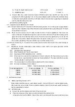
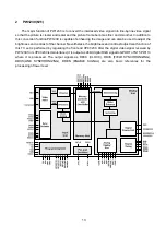
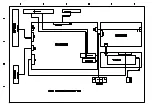
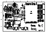
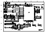
3 VPC3230(N10)
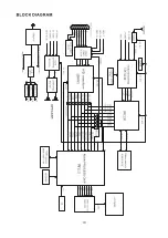
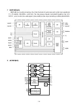
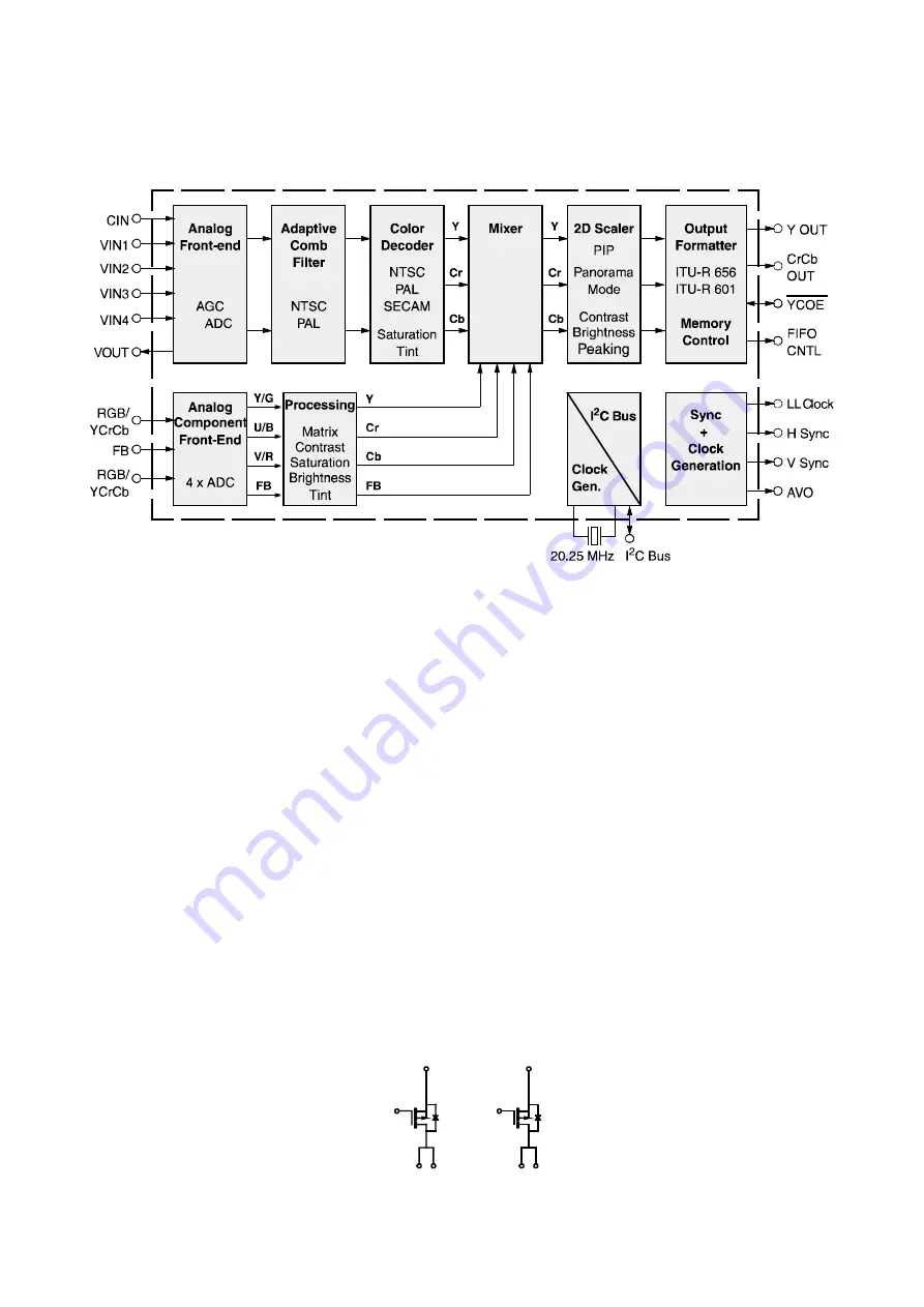
The block diagram of VPC3230 is shown as below:
2
In which:
71 pin CIN is signal input for S-VIDEO;
73 pin VIN2 is CVBS input for AV;
74 pinVIN3 is for TV signal input;
75 pinVIN4 is used for synchronous identification of YCRCB.
Pins 5,4,6 are respectively used for YCBCR signal input.
Pins 62 and 63 are connected to crystal oscillator of 20.25MHz and supply local frequency to
VPC3230.
Pins 13,14 are SAF AND SCL signals for bus line 12 to be used for communication with MCU
PW113.
VPC3230 that is used as video decoding chip sends the digital video signal in the format of
CCIR601, which is decoded from the analog video signal CVBS,S-VIDEO,YCBCR, to the deinterlacing
processor N11 PW1230 where conversion is made from interlace to non-interlace. VINCK, VHREF,
VINHS and VINVS sent out by VPC3230 are directly fed to PW1230.
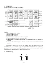
4 SI9933ADY(17)
S
1
G
1
D
D
1
1
P-C hannel M O SFE T
S
2
G
2
D
D
2
2
Summary of Contents for LC30B1
Page 1: ...COLOR TELEVISION LC30B1 ...
Page 12: ......
Page 14: ...12 ...
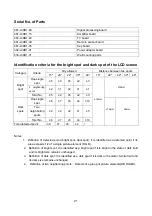
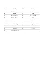
Page 19: ...17 9 K4S641632C N12 10 DS90C383A N16 D S 90C 383A D S 90C F383A ...
Page 20: ...18 11 Z86129 N8 ...
Page 21: ...19 12 LVC16244 N13 N14 13 PI5330 N1 14 74LV126 N4 ...
Page 22: ......
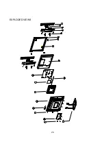
Page 28: ...26 EXPLODED VIEWS 1 2 3 4 5 6 7 8 9 10 11 12 13 14 15 16 17 18 19 ...
Page 30: ......
Page 31: ......
Page 32: ......
Page 33: ......
Page 34: ......
Page 35: ......
Page 36: ......


