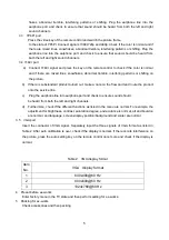
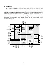
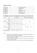
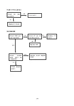
1
5
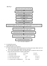
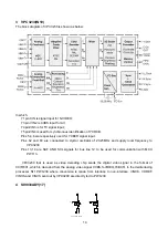
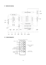
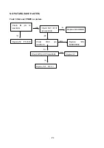
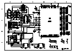
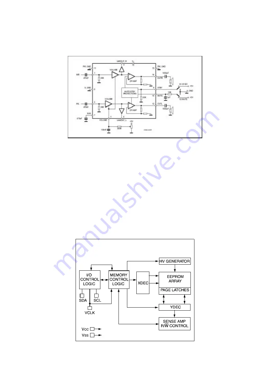
5 TDA7495(U601)
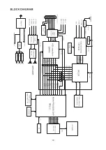
The block diagram of TDA7495 is shown below.
In which
Pins 1,5 are for input of left and right sound channels.
Pin 9 is control pin when STBY (valid when it is of low electric level).
Pin 10 is control pin for MUTE (valid when it is of high electric level).
Pin 13 is power supply pin for IC (24V).
Pins 12,14 are for power amplification output (output electric level is 10V).
For TDA7495, only when two control pins 9 and 10 are valid at the same time can there be sound
output. When servicing with power on please take care not to short circuit the IC pin or the power supply
because IC is liable to burnout.
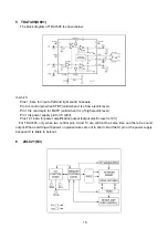
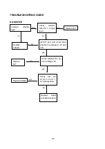
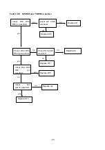
6 24LC21(N3)
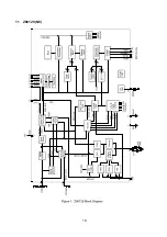
Summary of Contents for LC30B1
Page 1: ...COLOR TELEVISION LC30B1 ...
Page 12: ......
Page 14: ...12 ...
Page 19: ...17 9 K4S641632C N12 10 DS90C383A N16 D S 90C 383A D S 90C F383A ...
Page 20: ...18 11 Z86129 N8 ...
Page 21: ...19 12 LVC16244 N13 N14 13 PI5330 N1 14 74LV126 N4 ...
Page 22: ......
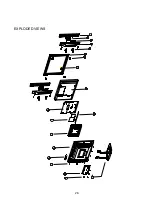
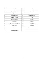
Page 28: ...26 EXPLODED VIEWS 1 2 3 4 5 6 7 8 9 10 11 12 13 14 15 16 17 18 19 ...
Page 30: ......
Page 31: ......
Page 32: ......
Page 33: ......
Page 34: ......
Page 35: ......
Page 36: ......


