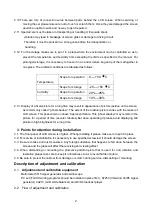
3
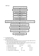
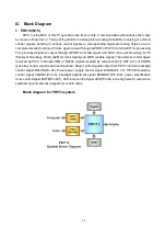
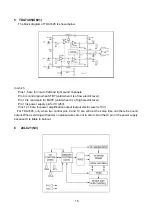
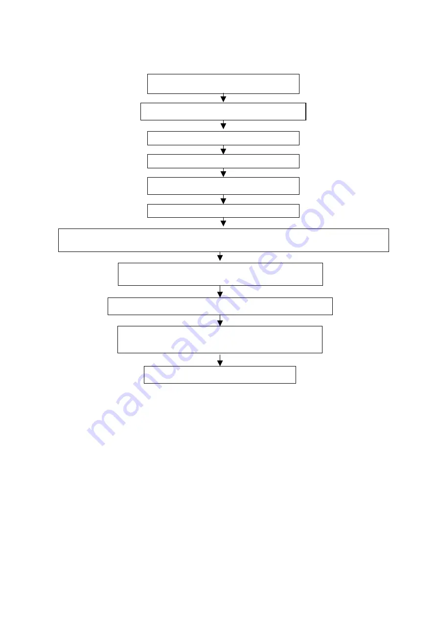
See Fig.1.
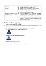
2.3 FLASH WRITE programs
FLASH WRITE memory N9.
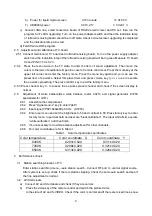
2.4 Main board adjustment and calibration
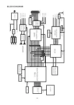
a) Connect main board to infrared receiving board, turn off the power supply adapter switch and
insert the plug of power supply adapter output into main board.
b) Turn on power supply adapter, check to see indication lamp in red light and check the power
supply and confirm various power supplies as listed below:
1) Main power supply C137 anode 5 V±0.2 V
2) Main power supply C138 3.3 V±0.1 V
3) PW1230 main power supply C142 2.5 V±0.1 V
4) PW113 main power supply L21 1.8 V±0.1 V
5) VPC3230 power for analog terminal L24 anode 5 V±0.2 V
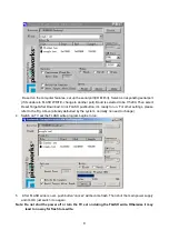
Check if memory U16 has been FLASH written.
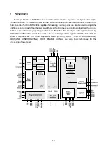
Production of main board and TV board on the line.
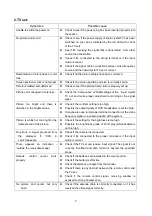
Check the main board
Check TV board
Combined test for general assembly
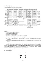
Connect to central signal source, check if various TV functions (station skipping, system identification, analog
control etc) are normal and check if earphone and speaker output are normal
Input AV/S signal and check various functions under AV/S terminal
Input VGA signal and check if display is normal in the state of PC
and various functions (analog control, line/field center etc.
Adjusting and calibrating TV board
Check accessories and then packing
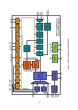
Fig.1 Flow process of adjustment
Input YprPb signal and check if display is normal in the state of PC
and various functions (analog control, line/field center etc
Summary of Contents for LC30B1
Page 1: ...COLOR TELEVISION LC30B1 ...
Page 12: ......
Page 14: ...12 ...
Page 19: ...17 9 K4S641632C N12 10 DS90C383A N16 D S 90C 383A D S 90C F383A ...
Page 20: ...18 11 Z86129 N8 ...
Page 21: ...19 12 LVC16244 N13 N14 13 PI5330 N1 14 74LV126 N4 ...
Page 22: ......
Page 28: ...26 EXPLODED VIEWS 1 2 3 4 5 6 7 8 9 10 11 12 13 14 15 16 17 18 19 ...
Page 30: ......
Page 31: ......
Page 32: ......
Page 33: ......
Page 34: ......
Page 35: ......
Page 36: ......


