background image

PDP

  TELEVISION

PH-42R6

Canada

Summary of Contents for PH-42R6

Page 1: ...PDP TELEVISION PH 42R6 Canada...

Page 2: ...tions Alignment instructions Working principle analysis of the unit Block diagram IC block diagram Wiring diagram Troubleshooting Schematic diagram APPENDIX A Main assembly list APPENDIX B Exploded vi...

Page 3: ...eat radiation parts or direct exposure to sunlight Otherwise there will be kickbacks 1 5 In case foreign substances such as water liquid metal slices or others fall into the module carelessly power mu...

Page 4: ...former On the other hand even if changes take place in the picture it can keep its brightness for a period of time several minutes It s a feature inherent with plasma and it s not abnormal However ple...

Page 5: ...ral signal source check if various TV functions station skipping modulate quantity control etc check if the output of earphone and speaker are normal Combined test for general assembly Input AV S sign...

Page 6: ...er power off for 10s 1 memory function after power off for 10s 0 no signal noise wave of TV 1 no signal blue screen of TV Bit2 1 00 STANDBY 01 turn on 10 memory function of turn on 00 complexion corre...

Page 7: ...VOL button to select AUTO COLOR 4 Performance check 4 1 TV function Input center source signal to RF TV terminal check if the channel is leak for auto searching 4 2 AV S and HDTV terminal Input AV S...

Page 8: ...l of 24bit to GM1501 1601 They sent to GM1501 1601 picture processing therein YPBPB or RGB to A D conversion after it and other three signal are switched selection and digital display processing it in...

Page 9: ...5V_STB VCC VBL Power_ON IR KeyA KeyB Led1 Led2 Mute HP_SW VGA_CAB DVI_CAB YUV VGA YUV_SW YUV USB Frame Buffer Frash ROM Video Decoder Video Decoder Deinterlacer HDMI RX Audio Processor Audio Switch L...

Page 10: ...cedures in order to achieve good stereo separation for BTSC and EIA J The MSP 34x0G has optimum stereo performance without any adjustments All MSP 34xxG versions are pin compatible to the MSP 34xxD On...

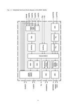
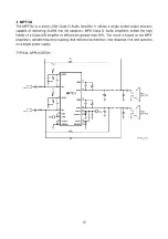
Page 11: ...9 Fig 1 1 Simplified functional block diagram of the MSP 34x0G...

Page 12: ...also available On CVBS and Y C inputs the user can control video characteristics such as hue contrast brightness and saturation via an I2C host port interface Furthermore luma peaking with programmab...

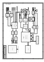
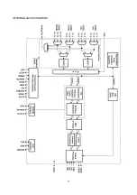
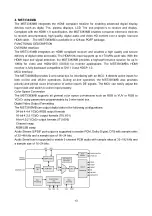
Page 13: ...11 INTERNAL BLOCK DIAGRAM...

Page 14: ...livering 2x20W into 4 speakers MPS Class D Audio Amplifiers exhibit the high fidelity of a Class A B amplifier at efficiencies greater than 90 The circuit is based on the MPS proprietary variable freq...

Page 15: ...backward compatible to DVI 1 0 and HDCP 1 0 MCU Interface The MST3383MB provides 2 wire serial bus for interfacing with an MCU It detects active inputs for both on line and off line operations During...

Page 16: ...ed onto a single device the gm1601H eliminates the need for several system components simplifying the design and reducing the cost of high end multimedia LCD monitors and televisions while maintaining...

Page 17: ...ipulation matrix supports all color spaces RGB YPrPb 4 4 4 YCrCb 4 2 2 YCr Cb ITU R BT656 ITU R BT601 Output supports analog RGB YPrPb and YCrCb in the FLI230x and digital RGB YPrPb 4 4 4 YCrCb and 4...

Page 18: ...luma and chroma video enhancer brings out details in the picture producing a more life like image 6 9 Memory 32 bit wide SDRAM i e one 2M x 32 bit or two 1M x 16 bit controller up to 166 MHz operatio...

Page 19: ...t of File C Documents and Settings PH42R6 Sch Drawn By TO KEYBOARD LVDS TO SPEAKER 8 PIN 12 PIN 6 PIN 11 PIN 12 PIN 10 PIN 6 PIN 667 PS42R6 53 667 PS42R6 56 POWER BOARD KEY BOARD XA9 XA7 XA5 X29 X13 X...

Page 20: ...e software again and check Power board problem Check the supply power D3 3V 12V Turn on the power again and check the power supply EEPROM abnormal Set the power to self turn on mode then check Turn of...

Page 21: ...ll other channels Check if the white balance of the factory menu is normal Refer to checking program4 Check if the X13 is signal wave If the panel lights or produce high voltage when turn on the TV Ch...

Page 22: ...check if input signal in sound power amplification board Measure if the sound input of the present channel is normal MSP3420 or other peripheral circuit have problem Check different levels of circuit...

Page 23: ...have problem N15 or the peripheral circuit have problem no yes no yes no yes Check if X7 have input signal Check if N7 has clock signal output and ITU R 656 is normal N7 and other peripheral circuit h...

Page 24: ...f the connection wire that directly corresponds to the position of the screen To judge these phenomena It s possible to check it by setting the screen to the state of self check as explained above Dia...

Page 25: ...lem still remains when the replacement is over then replace the logic board 5 There appears on the screen a mono color signal and one or several vertical bright lines of other colors a If it s a verti...

Page 26: ...Power board...

Page 27: ...Power board power board...

Page 28: ...2 501 LA3 STBL2012 501 LA9 STBL2012 501 LA6 STBL2012 501 LA11 STBL2012 501 23VSC CA7 100n CA47 470n CA46 470n CA102 100n GND D CA80 2 2n CA86 2 2n CA81 2 2n CA87 2 2n LOUT ROUT LOUT ROUT 9V GND D 5V_V...

Page 29: ...C282 100n C283 100n C284 100n C285 100n C286 100n C287 100n C288 100n C289 10uF 16V C290 10uF 16V C291 10uF 16V C292 10uF 16V C293 10uF 16V L47 STBL3216 601 L48 STBL3216 601 L49 STBL3216 601 L50 STBL...

Page 30: ..._1 54 Y_0 55 DVDD55 56 DGND56 57 C_9 FSO 58 C_8 BLUE 59 C_7 GREEN 60 C_6 RED 61 IOVDD61 62 IOGND62 63 C_5 64 C_4 65 C_3 66 C_2 67 DVDD67 68 DGND68 69 C_1 70 C_0 71 FID 72 HS CS 73 VS VBLK 74 XTAL1 75...

Page 31: ...OUT0 117 TEST OUT1 118 CTLOUT0 119 CTLOUT1 120 CTLOUT2 121 CTLOUT3 122 CTLOUT4 123 VDDcore6 1 8 124 VSScore 125 CLKOUT 126 B U b_OUT_0 127 B U b_OUT_1 128 VDD7 3 3 129 VSSio 130 B U b_OUT_2 131 B U b_...

Page 32: ...59 DQM3 60 A3 61 A4 62 A5 33 DQ17 34 DQ18 35 VDDQ35 36 DQ19 37 DQ20 38 VSSQ38 39 DQ21 40 DQ22 41 41 42 DQ23 43 VDD43 44 VSS44 58 VSS58 56 DQ31 55 VDDQ55 54 DQ30 53 DQ29 52 VSSQ52 51 DQ28 50 DQ27 49 V...

Page 33: ...D_GNDP12 P13 D_GNDP13 P14 D_GNDP14 P15 D_GNDP15 P16 D_GNDP16 P23 FS_2 5P23 P24 FSDATA10 FSDATA10 P25 FSDATA21 FSDATA21 P26 FSDATA11 FSDATA11 R1 ROM_CS ROM_CS R2 OCM_RE OCM_RE R3 OCM_WE OCM_WE R4 EXTC...

Page 34: ...MADDR 10 OCMADDR 0 19 OCMDATA 0 7 OCMADDR 18 OCMADDR 17 OCMADDR 16 OCMADDR 15 OCMADDR 14 OCMADDR 13 OCMADDR 12 OCMADDR 10 OCMADDR 9 OCMADDR 8 OCMADDR 7 OCMADDR 6 OCMADDR 5 OCMADDR 4 OCMADDR 3 OCMADDR...

Page 35: ...C244 47uF 10V C236 47uF 10V C241 47uF 10V C260 220u 10V L40 253D 02 C235 47uF 10V C237 100n C255 100n 3 3V X28 TJC3 11A 1 2 3 4 5 6 7 8 9 10 11 C346 100n L68 253D 02 C347 220u 10V 5VSTB C348 100n L69...

Page 36: ...381 10n L72 BG2012B300T R299 75 C379 10n L90 BG2012B300T C378 47uF 16V L73 BG2012B300T R298 75 R371 10K R301 75 YUV_SW 5V R319 10K C376 47uF 16V R322 10K R316 10K L89 BG2012B300T C374 47uF 16V R317 10...

Page 37: ...GND D C354 100n GND D GND D C419 100n R369 100 HD USB_SEL YUV_SW L_HD2 R_HD2 L_HD1 R_HD1 R41 100K R40 100K C320 1n L7 STBL2012 501 R42 1K L8 STBL2012 501 C269 100n C321 1n R43 1K AL_VGA AR_VGA X6 TJC...

Page 38: ...353 62494 20 MP7722DF 353 77220 10 CPU board 667 PS42R6 56 N15 N10 N7 N8 N34 GM1501 353 15010 60 FLI2310 353 23100 10 TVP5160 353 51600 10 TVP5147 353 51470 10 MST3383MB 353 33830 10 Keypad board 667...

Page 39: ...APPENDIX Exploded view PH 42X6...

Page 40: ...right 15 803 30206 00 upper Push board left 16 803 30204 00 leftPush board 17 Screen 18 870 3A121 00 ear frame leftupper rightbottom 19 870 10313 00 bracket right 20 870 3A122 00 ear frame rightupper...

Page 41: ...8 803 30208 00B bottom Push board left 39 803 30209 00B bottom Push board right 40 803 30205 00 rightPush board 41 877 60593 G0 button 42 Button board assy 43 360 30041 00 Power switch 44 870 10186 00...

Page 42: ...603 PH42R60 10 Ver 1 0...

Reviews: