
RESET#
HP_L
SIF1
HP_VOL
AL
AL
AR
AR
TV1
AV2
Y/AV1
C
SV_DET
SV_DET
VOUT
AV2
C
SV_DET
Y/AV1
HP_R
L_HD
L_HD
R_HD
R_HD
HP_R
HP_L
LOUT
ROUT
RESET#
MUTE
MUTE
VOUT
TV2
L1
R1
R2
R2
L2
AR
AL
L2
SIF2
SIGN1798
TV_MONO
SIF2
TV2
TV_MONO
SIF1
TV1
TV1
SRS_MONO
SRS_STE
SRS_STE
SRS_MONO
MUTE
HP_SW
SIGN1818
SIGN1804
L1
R1
R_HD
L_HD
+5V_RS232
CA60
470n
CA31
470p
CA78
1.5n
CA75
100n
CA54
1.5n
CA29
51p
CA50
470n
RA30
10K
GND-D
SCL
CA61
470n
CA79
470p
GND-D
CA57
470p
RA28
100
SDA
GND-D
CA53
470n
RA33
100
LA38
STBL2012-501
GND-D
SCL
GND-D
CA65
470n
RA56
100
GND-D
GND-D
RA75
10K
CA59
220p
SDA
RA45
100
+5V_A
CA56
470n
GND-D
RA34
100
CA27
51p
CA88
2.2n
LA37
STBL2012-501
GND-D
GND-D
CA37
100n
CA70
470n
CA112
100n
RA57
100
GND-D
RA74
10K
GND-D
GND-D
+5V_A
CA30
1.5n
CA58
470n
CA114
100n
GND-D
CA89
2.2n
LA36
STBL2012-501
CA28
51p
GND-D
CA111
100n
GA1
18.432MHz
DA1
LL4148
CA101
100n
NA3
1
NC
2
I2C_CL
3
I2C_DA
4
I2S-CL
5
I2S_WS
6
I2S_DA_OUT
7
I2S_DA_IN1
8
ADR_DA
9
ADR_WS
10
ADR_CL
11
DVSUP
12
DVSUP
13
DVSUP
14
DVSS
15
DVSS
16
DVSS
17
I2S_DA_IN2
18
NC
19
NC
25
DACA_L
26
VREF2
27
DACM_R
28
DACM_L
29
NC
30
DACM_SUB
31
NC
32
NC
33
SC2_OUT_R
34
SC2_OUT_L
35
VREF1
36
SC1_OUT_R
37
SC1_OUT_L
46
NC
47
SC4_IN_L
48
SC4_IN_R
49
ASG
50
SC3_IN_L
51
SC3_IN_R
52
ASG
53
SC2_IN_L
54
SC2_IN_R
55
ASG
56
SC1_IN_L
57
SC1_IN_R
58
VREFTOP
59
SCART_5_L
60
SCART_5_R/MONO
61
AVSS
62
AVSS
63
NC
64
NC
68
ANA_IN-
69
70
TESTEN
71
XTAL_IN
72
XTAL_OUT
73
TP
74
AUD_CL_OUT
75
NC
76
NC
77
D_CTR_I/O_1
78
D_CTR_I/O_0
79
ADR_SEL
80
STANDBYQ
20
NC
21
RESETQ
22
NC
23
NC
24
DACA-R
38
CAPL-A
39
AHVSUP
40
CAPL_M
41
NC
42
NC
43
AHVSS
44
AHVSS
45
AGNDC
65
AVSUP
66
AVSUP
67
+5V_A
NA7
TDA7053AT
1
NC
2
VC1
3
NC
4
VI1
5
VP
6
VI2
7
SGND
8
VC2
9
OUT2+
10
PGND
11
NC
12
OUT2-
13
OUT1-
14
PGND
15
NC
16
OUT1+
CA94
1n
CA96
1n
GND-D
CA132
100n
CA133
100n
+5V_V
RA43
10K
+23V_AMP
CA127
100n
CA126
100n
GND-D
+12V
LA24
STPB3216-380PT
LA42
253D-02
LA35
253D-02
LA40
GND-D
+5V_A
CA104
1u
CA90
1u
CA91
1u
RA64
3.3K
LA16
68uH
LA21
68uH
CA25
18p
CA26
18p
GND-D
RA7
100K
RA5
100K
RA6
100K
CA10
1n
RA11
1K
GND-D
GND-D GND-D
GND-D
CA9
1n
RA10
1K
RA15
470
RA16
470
RA13
1K
RA14
1K
VA1
BC847AW
VA2
BC847AW
CA19
100n
GND-D
GND-D
GND-D
CA130
1000u
16V
CA118
1000u
16V
CA117
1000u
16V
RA19
75
RA26
1K
RA18
75
CA22
1n
RA21
100K
RA27
1K
RA24
1K
RA25
1K
RA22
100K
RA23
100K
RA20
100K
CA8
100n
NA2
PACDN045YB6
1
2
3
4
5
6
GND-D
CA23
1n
CA20
1n
CA21
1n
GND-D
RA17
75
XA3
CKX5-2K-2
Y
C
CA134
470u
35V
CA121
470u
35V
XA1
AV3-14WKD
Y
W
R
XA2
AV3-14WKD
Y
W
R
XA4
AV3-14WKD
Y
W
R
GND-D
GND-D
GND-D
GND-D
GND-D
GND-D
GND-D
GND-D
GND-D
GND-D
GND-D
GND-D
GND-D
GND-D
GND-D
GND-D
GND-D
GND-D
GND-D
GND-D
GND-D
GND-D
GND-D
+9V
XA10
CKX3-3.5-1K
R
L
GND-D
RA8
75
GND-D
RA9
75
LA17
68uH
NA1
PACDN045YB6
1
2
3
4
5
6
LA10
STBL2012-501
LA5
STBL2012-501
LA12
STBL2012-501
LA1
STBL2012-501
LA7
STBL2012-501
LA2
STBL2012-501
LA8
STBL2012-501
LA3
STBL2012-501
LA9
STBL2012-501
LA6
STBL2012-501
LA11
STBL2012-501
+23VSC
CA7
100n
CA47
470n
CA46
470n
CA102
100n
GND-D
CA80
2.2n
CA86
2.2n
CA81
2.2n
CA87
2.2n
LOUT
ROUT
LOUT
ROUT
+9V
GND-D
+5V_V
RA1
100
RA3
100
CA12
100n
SCL
CA4
100n
+5V_V
CA1
100n
SDA
LA43
LA48
68uH
LA45
68uH
SDA
LA44
SCL
RA4
100
RA2
100
CA5
100n
RA12
75
+5V_V
CA13
100n
CA15
10n
+5V_V
CA2
100n
LA46
68uH
LA47
68uH
XA5
1
2
3
4
5
6
XA9
TJC10-08A
1
2
3
4
5
6
7
8
XA7
TJC10-12A
1
2
3
4
5
6
7
8
9
10
11
12
+9V
RA29
100
CA73
47u
35V
DA2
LL4148
GND-D
VA3
BC847AW
RA46
10K
CA122
100n
RA48
100
RA52
10K
RA51
4.7K
CA115
1000u
35V
GND-D
VA5
BC847AW
CA110
1000u
35V
RA49
10K
VA4
BC857AW
RA55
10K
GND-D
GND-D
GND-D
RA41
10K
CA119
100n
CA107
22p
GND-D
CA137
1000u
35V
CA95
10n
GND
GND-D
CA108
1u
CA136
470n
CA103
22p
DA9
BZV55-B6V2
RA58
10K
RA65
82K
+23V_AMP
RA66
82K
LA51
STPB3216-380PT
RA70
10
RA72
10K
CA100
10n
GND
GND
RA69
10
RA63
100K
GND-D
RA77
10
GND-D
CA139
100n
CA105
470u
35V
CA109
1u
RA76
10
LA54
DASL983BN-1003
CA138
1000u
35V
GND-D
RA62
100K
CA84
1u
RA54
100K
CA106
470u
35V
CA116
100n
GND-D
CA140
100n
DA8
BZV55-B6V2
GND-D
GND-D
CA85
1u
RA60
100K
CA135
470n
LA52
STPB3216-380PT
GND
XA12
1
2
3
4
CA125
390p
GND-D
GND
+23V_AMP
RA61
100K
RA73
10K
LA55
DASL983BN-1003
RA53
100K
RA59
10K
GND
CA124
390p
CA44
100n
RA35
2K
CA72
10n
RA42
3K
CA33
10n
GND-D
+9V
CA64
100n
GND-D
GND-D
LA49
68uH
CA42
4.7n
RA44
1.5K
RA38
100
CA66
18n
CA45
100n
NA5
M62494FP
1
RIN
2
LIN
3
SRS PR
4
SRS A
5
ROUT
6
SRS NR
7
SRS NL
8
LOUT
9
Vcc
10
Mute
11 SRS MONO
12 SRS STEREO
13 GND
14 PS
15 LPF
16 HPF
17 BPF
18 L+R
19 REF IN
20 REF OUT
CA67
470p
CA38
100n
RA36
3.9K
RA37
100
CA68
470p
CA32
100n
CA43
220n
CA71
820n
GND-D
RA50
0
RA47
0
CA123
470u
35V
CA51
100n
XA6
1
2
3
4
NA4
MAX3232CSE
1
C1+
2
V+
3
C1-
4
C2+
5
C2-
6
V-
7
T2OUT
8
R2IN
9
R2OUT
10
T2IN
11
T1IN
12
R1OUT
13
R1IN
14
T1OUT
15
GND
16
Vcc
CA34
47p
CA52
100n
RA39
100
CA55
22u
16V
RA32
100
RA31
1K
RA40
100
CA35
47p
CA49
100n
CA40
100n
CA39
100n
XA11
TJC3-10A
1
2
3
4
5
6
7
8
10
9
NA6
MP7722
1
NC1
2
REF1
3
IN1
4
AGND1
5
NC5
6
EN1
7
IN2
8
REF2
9
AGND2
10
EN2
11
NC11
12
BS2
13
VDD2
14
SW2
15
PGND2
16
NC16
17
BS1
18
VDD1
19
SW1
20
PGND1
AMP_VCC2
AMP_VCC2
AMP_VCC1
AMP_VCC1
CA92
10u
16V
CA93
10u
16V
DA5
LL4148
DA4
LL4148
RA67
20K
RA68
20K
TUNA1
JS-6AM/134-A2
1
VCC3
2
BT
3
VCC1
5
SDA
6
AS
11
SIF
4
SCL
12
VIDEO
13
VCC2
14
AUDIO
7
AFC
TUNA2
JS-6AM/134
1
AGC
2
BT
3
VCC1
5
SDA
6
AS
11
SIF
4
SCL
12
VIDEO
13
VCC2
14
AUDIO
7
AFC
CA16
470u
16V
CA18
10u
16V
CA17
10u
16V
CA3
220u
16V
CA6
220u
16V
CA11
220u
16V
CA14
220u
16V
CA24
47u
16V
CA36
10u
16V
CA41
10u
16V
CA48
47u
16V
CA62
2.2u
50V
CA63
2.2u
50V
CA69
100u
16V
CA74
3.3u
50V
CA77
47u
16V
CA82
10u
16V
CA83
10u
16V
CA99
470u
16V
CA128
47u
16V
CA129
47u
16V
NA8
TA78M09P
OUT
INPUT
GND
CA131
100n
XA8
7906-9F
1
2
3
4
5
6
7
8
9
10
11
CA76
470u
35V
LA50
253D-02
DA3
LL4148
+5V_A
DA10
SK34A
DA7
SK34A
DA11
SK34A
DA6
SK34A
CA141
100n
LA56
68uH
+9V
RA78
0
+5V
+5V
CA98
4700p
CA97
4700p
+5V_RS232
+5V_RS232
2005.06.22
Ver1.0
(ADDR:80H)
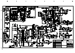
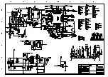
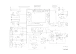
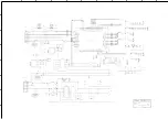
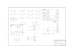
MSP3420
L
R
RXD
RXD
TXD
TXD
VCC
TXD
RXD
GND
782-PH42R7-5300
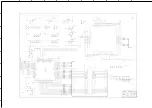
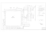
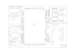
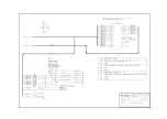
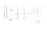
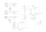
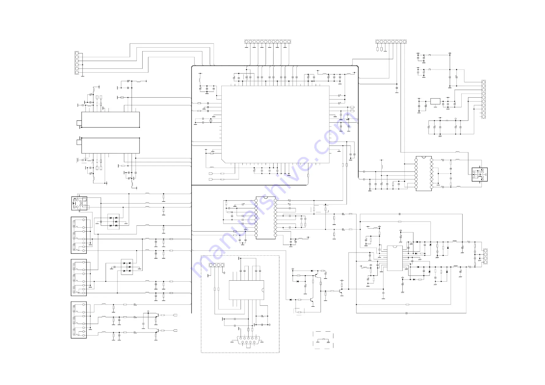
Analog board
Summary of Contents for PH-42R6
Page 1: ...PDP TELEVISION PH 42R6 Canada...
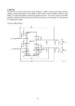
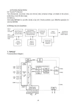
Page 11: ...9 Fig 1 1 Simplified functional block diagram of the MSP 34x0G...
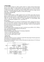
Page 13: ...11 INTERNAL BLOCK DIAGRAM...
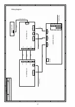
Page 26: ...Power board...
Page 27: ...Power board power board...
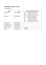
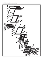
Page 39: ...APPENDIX Exploded view PH 42X6...
Page 42: ...603 PH42R60 10 Ver 1 0...


