
XOCECO
REV.
Sheet to
TITLE:
DWG NO.
Date:
7
1
A1.0
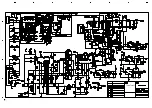
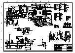
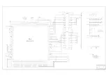
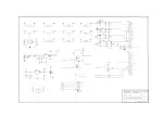
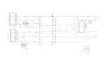
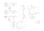
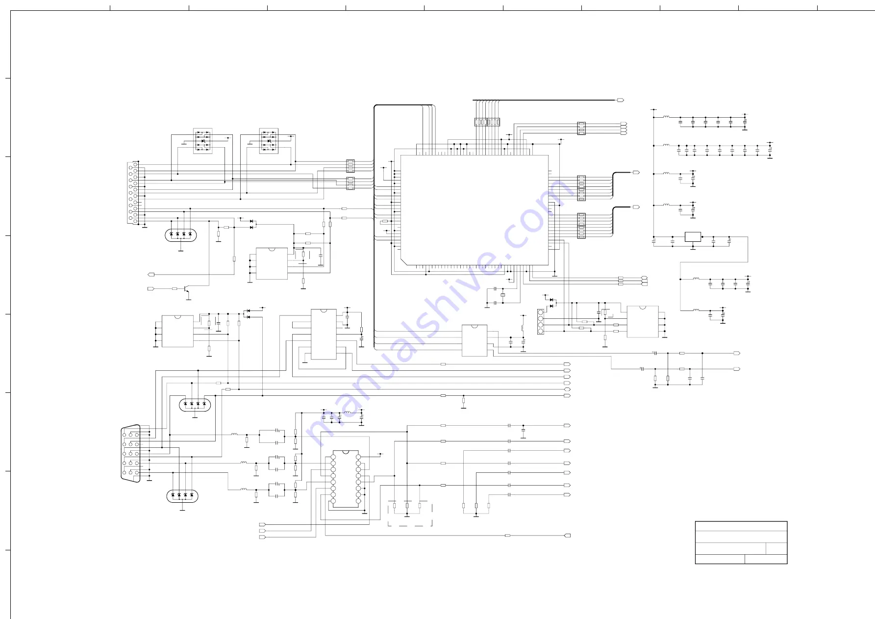
CPU
203-L37R70-01DL
版
年
月
日
XIAMEN OVERSEAS CHINESE
ELECTRONIC CO., LTD.
N34
MST3383MB
NOT TO BE POPULATED
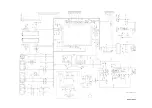
HDMI EDID
VGA EDID
HDMI PORT
VGA PORT
HDCP KEY
A-GREEN
A-RED
A-BULE
Pr
Y
Pb
VGRN[7-0]
VGRN[7]
VGRN[6]
VGRN[5]
VGRN[4]
VGRN[3]
VGRN[2]
VGRN[1]
VGRN[0]
VRED[7-0]
VRED[7]
VRED[6]
VRED[5]
VRED[4]
VRED[3]
VRED[2]
VRED[1]
VRED[0]
DDCSCL
DDCSDA
RX0+
RX1+
RX2-
RX2+
RXCK-
RXCK+
MCLK
LRCK
SCLK
SDATA
AR_HDMI
MCLK
LRCK
SCLK
SDATA
RX0-
RX1-
DDCSCL
DDCSDA
VBLU[7]
VBLU[0]
VBLU[1]
VBLU[2]
VBLU[3]
VBLU[4]
VBLU[5]
VBLU[6]
AL_HDMI
HDMI_5V
HDMI(DVI)_CAB
RX2-
RX2+
RX0-
RX0+
RX1-
RX1+
RXCK-
RXCK+
RX1-IN
RX1+IN
RXCK-IN
RXCK+IN
RX2+IN
RX2-IN
RX0+IN
RX0-IN
R14
100
R15
100
R5
100
R16
10K
R17
10K
VGA_CAB
VGA_SCL
R22
100K
D1
MMBD1204
VGA_SDA
R10
10K
R12
10K
X3
HDR-F15S-3
1
23
4
5
67
89
11
12
13
14
10
15
R6
100
R24
10K
R32
100K
C16
10n
C17
10n
C18
10n
C19
10n
C20
10n
C21
10n
C22
10n
R26
20
R27
20
R28
20
R20
75/1%
R21
75/1%
R23
75/1%
SOG
BLUE+
BLUE-
GREEN+
GREEN-
RED+
RED-
RGB/YPbPr_SEL
C2
100n
C15
100n
C6
100n
C10
100n
C4
100n
C11
100n
C5
100n
L2
BG2012B300T
L1
BG2012B300T
L3
BG2012B300T
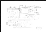
AHS
AVS
+5V
+5V_MUX
R29
100
+5V
C12
100uF
16V
C13
100uF
16V
D2
MMBD1204
R3
10K
R18
10K
+5V
C9
47uF
10V
C7
47uF
10V
C8
47uF
10V
R4
0
R19
0
N1
24C02N-10SI27
1
AO
2
A1
3
A2
4
GND
5
SDA
6
SCL
7
WP
8
Vcc
X2
HDMI
18
11
4
17
7
14
3
2
10
13
6
19
9
1
16
5
12
15
8
N4
PI5V330
1
IN
2
S1A
3
S2A
4
DA
5
S1B
6
S2B
7
DB
8
GND
9
DC
10
S2C
11
S1C
12
DD
13
S2D
14
S1D
15
/EN
16
VCC
N24
SN74AHC14PWR
1
1A
2
1Y
3
2A
4
2Y
5
3A
6
3Y
7
GND
8
4Y
9
4A
10
5Y
11
5A
12
6Y
13
6A
14
VCC
N5
24LC04
1
AO
2
A1
3
A2
4
GND
5
SDA
6
SCL
7
WP
8
Vcc
R8
75
R9
75
R7
75
R189
10K
R190
10K
R191
10K
R192
10K
R193
10K
R194
10K
+5V_MUX
+3.3V_DIG
C1
47uF
FLS_DET
C14
100n
R2
330K
C3
47p
R11
10K
+5V
+5V
HDMI(DVI)_CAB
R212
100
R213
100
R214
10
R215
10
R216
10
R217
10
R218
10
R219
10
VGRN[7-0]
VRED[7-0]
VBLU[7-0]
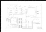
G5
14.31818MHz
C263
22p
C264
22p
SW_SCL
SW_SDA
C265
3.9n
C266
3.9n
C267
10uF
16V
C268
10uF
16V
R36
10K
R37
10K
R39
470
R38
470
V_AUPLL
V_PLL
V_MPLL
V_DDC
V_DDP
C270
100n
C271
100n
C272
100n
C273
100n
C274
100n
C275
100n
C276
100n
C277
100n
C278
100n
C279
100n
C280
100n
C281
100n
C282
100n
C283
100n
C284
100n
C285
100n
C286
100n
C287
100n
C288
100n
C289
10uF
16V
C290
10uF
16V
C291
10uF
16V
C292
10uF
16V
C293
10uF
16V
L47
STBL3216-601
L48
STBL3216-601
L49
STBL3216-601
L50
STBL3216-601
L51
STBL3216-601
L52
STBL3216-601
C294
10uF
16V
V_MPLL
V_PLL
V_DDP
V_DVI
V_DDC
V_AUPLL
3V3SC
N32
AS1117-2V5
IN
OUT
C295
47uF
10V
C296
47uF
10V
C297
100n
C298
100n
R220
390
RESET_OUT
R221
100
3V3SC
R222
0
C299
100n
V_DVI
R223
10
L53
STBL3216-601
C300
100n
C301
10uF
16V
+5V
VVS
VHS
VCLK
R234
100
VDE
L4
68uH
R33
56
R34
56
R35
56
N2
24C02N-10SI27
1
AO
2
A1
3
A2
4
GND
5
SDA
6
SCL
7
WP
8
Vcc
R235 10K
R236
4.7K
R237
4.7K
1
NC1
2
NC2
3
NC3
4
AVDD_DVI4
5
GND5
6
NC6
7
NC7
8
NC8
9
NC9
10
NC10
11
NC11
12
NC12
13
NC13
14
NC14
15
NC15
16
NC16
17
NC17
18
NC18
19
NC19
20
NC20
26
NC26
27
NC27
28
NC28
29
AVDD_DVI29
30
GND30
31
GND31
32
AVDD_MPLL
33
XOUT
34
XIN
35
HWRESET
36
A0
37
SCL
38
SDA
39
VDDP39
40
INT
41
MCL
42
MDA
43
DATA[23]
44
DATA[22]
45
DATA[21]
56
DATA[14]
57
DATA[13]
58
DATA[12]
59
DATA[11]
60
DATA[10]
61
DATA[9]
62
DATA[8]
63
NC63
64
NC64
65
VDDP65
66
GND66
67
VDDC67
68
DATACK
69
SOGOUT/DE
70
HSOUT
71
VSOUT
72
FIELD/GPO
73
VDDP73
74
GND74
75
VDDC75
81
DATA[2]
82
DATA[1]
83
DATA[0]
84
NC84
85
NC85
86
VDDP86
87
GND87
88
VDDP88
89
GND89
90
VDDP90
91
GND91
92
VDDC92
93
NC93
94
NC94
95
NC95
96
AUSD
97
AUSCK
98
AUWS
99
AUMUTE
100
MCKO
21
NC21
22
NC22
46
DATA[20]
47
DATA[19]
54
GND54
55
DATA[15]
79
DATA[4]
80
DATA[3]
23
NC23
24
NC24
25
NC25
48
DATA[18]
49
DATA[17]
50
DATA[16]
51
NC51
52
NC52
53
VDDP53
76
DATA[7]
77
DATA[6]
78
DATA[5]
101
SPDIFO
102
VDDP102
103
GND103
104
GND104
105
GND105
106
AVDD_AUPLL
107
GND107
108
RX0N
109
RX0P
110
GND110
111
RX1N
112
RX1P
113
AVDD_DVI113
114
RX2N
115
RX2P
116
GND116
117
RXCKN
118
RXCKP
119
AVDD_DVI119
120
REXT
121
NC121
122
GND122
123
AVDD_PLL
124
DDCSCL
125
DDCSDA
126
AVDD_DVI126
127
GND127
128
NC128
R238
100
R239
100
V17
BC847AW
HDMI_RST
R240
2.2K
D9
MMBD1204
R245
1K
X22
1
2
3
4
R251
10
R252
10
R209
100
R210
100
Pb
Y
Pr
AR_HDMI
AL_HDMI
R25
750
N26
CS4334
1
SDATA
2
SCLK/DEM
3
LRCK
4
MCLK
5
AOUTR
6
AGND
7
VA
8
AOUTL
N28
PESD5V0L4UG
1
2
3
4
5
N27
PESD5V0L4UG
1
2
3
4
5
N31
PESD5V0L4UG
1
2
3
4
5
N29
PRTR5V0U4D
1
2
3
4
5
6
N30
PRTR5V0U4D
1
2
3
4
5
6
5
2,3
2,3
5
3,5
5
3,5
3,5
3,5
3,5
3,5
5
5,7
5,7
5
5
5
5
5
5
5
5
5
5
5
5
8
8
8
9
9
A
B
C
D
E
F
G
H
I
1
2
3
4
5
6
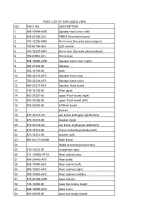
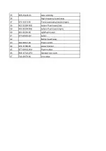
Summary of Contents for PH-42R6
Page 1: ...PDP TELEVISION PH 42R6 Canada...
Page 11: ...9 Fig 1 1 Simplified functional block diagram of the MSP 34x0G...
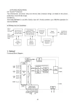
Page 13: ...11 INTERNAL BLOCK DIAGRAM...
Page 26: ...Power board...
Page 27: ...Power board power board...
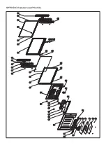
Page 39: ...APPENDIX Exploded view PH 42X6...
Page 42: ...603 PH42R60 10 Ver 1 0...


