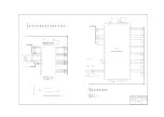

XOCECO
REV.
Sheet to
TITLE:
DWG NO.
Date:
N7
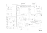
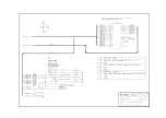
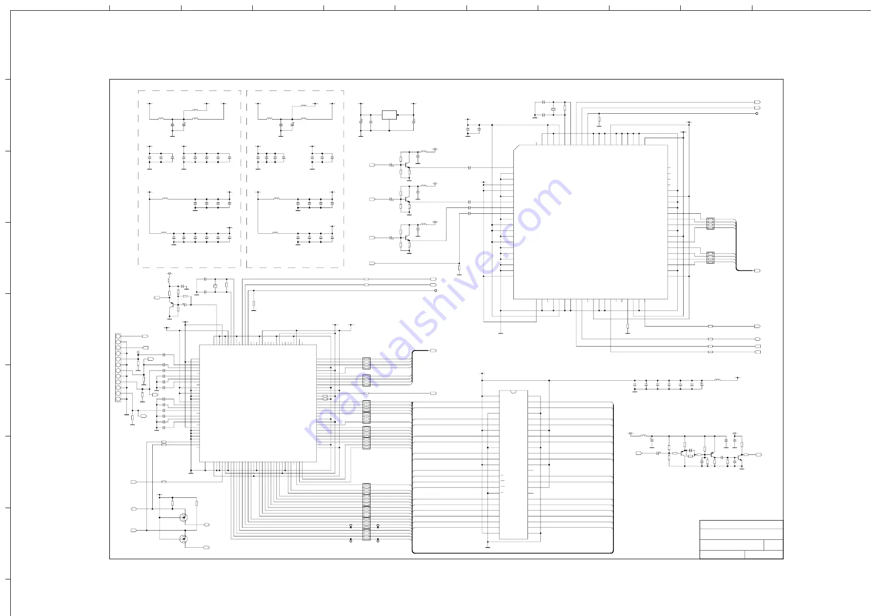
TVP5160
7
2
A1.0
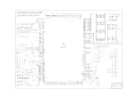
CPU
203-L37R70-01DL
Video Decoders
版
年
月
日
XIAMEN OVERSEAS CHINESE
ELECTRONIC CO., LTD.
DECOUPLING FOR TVP5160
DECOUPLING FOR TVP5147
SW_SCL
SV[7]
/RESET
SW_SDA
SVCLK
SV[3]
SV[2]
SV[1]
SV[0]
SV[6]
SV[5]
SV[4]
DEC_CLK
PDEC_A1.8V
DEC_Y[0]
DEC_Y[1]
DEC_Y[2]
DEC_Y[3]
DEC_Y[4]
DEC_Y[5]
DEC_Y[7]
DEC_Y[6]
DECSDA[3]
DECSDA[2]
DECSDA[1]
DECSDA[10]
DECSDBA0
DECSDRAS#
DECSDCAS#
DECSDWE#
DECSDA[4]
DECSDA[5]
DECSDA[6]
DECSDA[7]
DECSDA[8]
DECSDA[9]
DECSDCLK
DECSDDQM
DECSDD[8]
DECSDD[9]
DECSDD[11]
DECSDD[12]
DECSDD[13]
DECSDD[14]
DECSDD[15]
DECSDD[7]
DECSDD[6]
DECSDD[5]
DECSDD[4]
DECSDD[3]
DECSDD[2]
DECSDD[1]
DECSDD[0]
DECSDD[15]
DECSDD[13]
DECSDD[11]
DECSDD[9]
DECSDD[8]
DECSDCLK
DECSDDQM
DECSDA[8]
DECSDA[7]
DECSDA[6]
DECSDA[5]
DECSDA[4]
DECSDD[7]
DECSDWE#
DECSDRAS#
DECSDD[10]
DECSDA[2]
SHS
SVS
DECSDA[3]
DECSDA[1]
DECSDA[0]
DECSDD[0]
DECSDD[1]
DECSDD[2]
DECSDD[3]
DECSDD[4]
DECSDD[5]
DECSDD[6]
DECSDDQM
DECSDCAS#
DECSDA[9]
DECSDD[12]
DECSDBA0
DECSDD[14]
DECSDD[10]
DECSDA[10]
DECSDA[0]
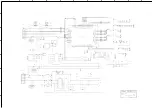
VOUT
Y_PIP
Y/AV1
AV2
C
+5V
+5V
TV2
VOUT
+5V
HS_COUNTER
TV2
VOUT
+12V
C33
33p
C32
33p
G1
14.31818MHz
R54
100K
DEC_VS
DEC_HS
R57
10K
R59
10K
R63
100
R64
100
R65
100
/RESET
R61
10K
SV[7-0]
R60
10K
R68
100
/RESET
G2
14.31818MHz
SVCLK
R69
100
SW_SCL
R55
100K
C34
33p
R67
100
C35
33p
DEC_Y[7-0]
N9
AS1117-1V8
IN
OUT
R56
2.7K
R58
2.7K
SW_SCL
MSTR_SDA
MSTR_SCL
SVS
SHS
R77
22
R62
22
R76
22
R66
22
R72
22
R75
22
R73
22
R74
22
C24
100n
C62
100n
C31
100n
C54
100n
C57
100n
C37
100n
C47
100n
C55
100n
C46
100n
C53
100n
C49
100n
C45
100n
C67
100n
C48
100n
C56
100n
C50
100n
C65
100n
C63
100n
C66
100n
C61
100n
C25
100n
C69
100n
C23
100n
C27
100n
C41
100n
C40
100n
C43
100n
C26
100n
C64
100n
C59
100n
C58
100n
C51
100n
C39
100n
C52
100n
C68
100n
C42
100n
C71
100n
C30
100n
C36
100n
C60
100n
TP1
TP2
DEC_CLK
R50
75
R49
75
R44
75
R45
75
C28
100n
C29 100n
MDEC_A3.3V
MDEC_A1.8V
3V3SC
MDEC_D1.8V
MDEC_D3.3V
3V3SC
MDEC_A3.3V
MDEC_D3.3V
MDEC_D3.3V
MDEC_A3.3V
+1.8VDEC
MDEC_A1.8V
MDEC_D1.8V
PDEC_A3.3V
3V3SC
PDEC_D3.3V
C38
100uF
10V
C44
100uF
10V
PDEC_A3.3V
PDEC_D3.3V
PDEC_A1.8V
+1.8VDEC
PDEC_D1.8V
PDEC_A3.3V
PDEC_A1.8V
3V3SC
+1.8VDEC
PDEC_D1.8V
PDEC_D3.3V
V2
BSS138LT1
G
D
S
V1
BSS138LT1
G
D
S
L10
STBL3216-601
L17
STBL3216-601
L18
STBL3216-601
L14
STBL3216-601
L13
STBL3216-601
L12
STBL3216-601
L9
STBL3216-601
L11
STBL3216-601
L16
STBL3216-601
L15
STBL3216-601
C72
47uF
10V
C70
47uF
10V
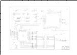
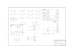
N8
TVP5147PFP
1
VI_1_B
2
VI_1_C
3
CH1_A33GND
4
CH1_ASSVDD
5
CH2_ASSVDD
6
CH2_A33GND
7
VI_2_A
8
VI_2_B
9
VI_2_C
10
CH2_A18GND
11
CH2_A18VDD
12
A18VDD_REF
13
A18GND_REF
14
NC14
15
NC15
16
VI_3_A
17
VI_3_B
18
VI_3_C
19
NC19
20
NC20
21
NC21
22
NC22
23
VI_4_A
24
CH4_A18GND
25
CH4_A18VDD
26
NSUB
27
TMS
28
SCL
29
SDA
30
INTREQ
31
DVDD
32
DGND
33
PWDN
34
RESETB
35
FSS
36
AVID
37
GLCL/I2CA
38
IOVDD38
39
IOGND39
40
DATACLK
41
DVDD41
42
DGND42
43
Y_9
44
Y_8
45
Y_7
46
Y_6
47
Y_5
48
IOVDD48
49
IOGND49
50
Y_4
51
Y_3
52
Y_2
53
Y_1
54
Y_0
55
DVDD55
56
DGND56
57
C_9/FSO
58
C_8/BLUE
59
C_7/GREEN
60
C_6/RED
61
IOVDD61
62
IOGND62
63
C_5
64
C_4
65
C_3
66
C_2
67
DVDD67
68
DGND68
69
C_1
70
C_0
71
FID
72
HS/CS
73
VS/VBLK
74
XTAL1
75
XTAL2
76
PLL_A18VDD
77
ALL_A18GND
78
CH1_A18VDD
79
CH1_A18GND
80
VI_1_A
1
A33GND1
2
A33VDD2
3
VI_1
4
VI_2
5
VI_3
6
NC
7
VI_4
8
VI_5
9
VI_6
10
NC
11
A18VDD11
12
A18GND12
13
A18VDD13
14
A18GND14
15
A18GND15
16
A18VDD16
17
VI_7
18
VI_8
19
VI_9
20
NC20
26
A33GND26
27
A33GND27
28
NSUB
29
TMS
30
SCL
31
SDA
32
INTREQ
33
DVDD33
34
DGND34
35
PWDN
36
RESETB
37
IOVDD37
38
IOGND38
39
D0
40
D1
41
D2
42
D3
43
D4
44
D5
45
D6
56
D8
57
IOVDD57
58
IOGND58
59
DQM
60
CLK
61
A11
62
A9
63
A8
64
A7
65
DVDD65
66
DGND66
67
A6
68
A5
69
A4
70
WE#
71
CAS#
72
RAS#
73
BA0
74
IOVDD74
75
IOGND75
81
A3
82
GPIO/I2CA1
83
GLCO/GPIO/I2CA0
84
DATACLK
85
DVDD85
86
DGND86
87
Y_9
88
Y_8
89
Y_7
90
Y_6
91
Y_5
92
IOVDD92
93
IOGND93
94
Y_4
95
Y_3
96
Y_2
97
Y_1
98
Y_0
99
DVDD99
100
DGND100
21
VI_10
22
VI_11
46
D7
47
DVDD47
54
D10
55
D9
79
A1
80
A2
23
VI_12
24
NC24
25
A33VDD25
48
DGND48
49
D15
50
D14
51
D13
52
D12
53
D11
76
BA1
77
A10
78
A0
101
C_9/GPIO/FSO
102
C_8/GPIO/BLUE
103
C_7/GPIO/GREEN
104
C_6/GPIO/RED
105
IOVDD105
106
IOGND106
107
C_5/GPIO
108
C_4/GPIO
109
C_3/GPIO
110
C_2/GPIO
111
DVDD111
112
DGND112
113
C_1/GPIO
114
C_0/GPIO
115
AVID/GPIO
116
FID/GPIO
117
HS/CS/GPIO
118
VS/VBLK/GPIO
119
FSS
120
AGND
121
XIN
122
XOUT
123
PLL18VDD
124
PLL18GND
125
A33VDD125
126
A33GND126
127
ANALOG_OUT
128
A33GND128
129
PP
C302
100n
C303
100n
C304
100n
C305
100n
C306
100n
C307
100n
C308
100n
C309
100n
C310
100n
C311
100n
R224
10K
V_SDRAM2
C312
100n
C313
47uF
10V
C314
100n
C315
100n
C316
100n
C317
100n
C318
100n
C319
100n
L54
STPB3216-380PT
3V3SC
SW_SDA
SW_SDA
R233
22
R232
22
R226
22
R228
22
R229
22
R230
22
R231
22
R225
22
R227
22
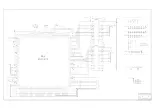
N33
K4S161622D-TI/E
40
DQ9
1
VDD1
11
DQ6
49
DQ15
3
DQ1
8
DQ4
6
DQ3
48
DQ14
41
VSS41
47
VSSQ47
7
VDDQ7
5
DQ2
44
VDD44
9
DQ5
42
DQ10
10
VSSQ10
43
DQ11
4
VSSQ4
45
DQ12
50
VSS50
2
DQ0
46
DQ13
12
DQ7
39
DQ8
13
VDDQ13
14
LDQM
37
NC37
38
VDD38
15
WE
36
DQMU
16
CAS
35
CLK
17
RAS
18
CS
33
NC
34
CKE
19
BA
20
AP
31
A8
32
A9
21
A0
30
A7
22
A1
23
A2
24
A3
27
A4
28
A5
29
A6
25
VDD25
26
VSS26
X7
TJC10-12A
1
2
3
4
5
6
7
8
9
10
11
12
R279
220
R280
0
R281
10K
C365
100n
V26
BC857AW
C364
47uF
16V
+5V
R282
22K
L65
STBL2012-221
VOUT
VOUT
C
Y/AV1
AV2
TV1
C339
100n
V23
BC847AW
V24
BC847AW
V25
BC847AW
C340
47uF
16V
C341
47uF
16V
C342
47uF
16V
R269
10K
R270
10K
R271
10K
R272
22K
R273
22K
R274
22K
R275
470
R276
470
R277
470
Y/AV1
AV2
C
L58
STBL2012-221
L59
STBL2012-221
L60
STBL2012-221
+5V
+5V
+5V
C343
100n
C344
100n
C345
100n
TV2
R278
75
C366
10uF
C370
100n
GND-D
GND-D
L66
STBL2012-501
V28
BC857AW
C371
100n
C372
1.5n
R284
10K
R293
10K
R286
1K
C368
1.5n
R285
1K
R291
12K
GND-D
C367
1u
GND-D
R287
560K
R288
560
R292
10K
R289
560K
R294
100
C369
560p
C353
100uF
16V
V29
BC847AW
R290
15K
R283
10K
VOUT
V27
BC857AW
HS_COUNTER
TV2
+5V
+12V
TP18
1
TP20
1
TP19
1
TP21
1
(BB/BA)
(B9/B8)
5
5
3,5
1,3
1,3
5
5
5
5
1,3
1,3
3,5
3
3
3
3
5
A
B
C
D
E
F
G
H
I
1
2
3
4
5
6
7
Summary of Contents for PH-42R6
Page 1: ...PDP TELEVISION PH 42R6 Canada...
Page 11: ...9 Fig 1 1 Simplified functional block diagram of the MSP 34x0G...
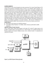
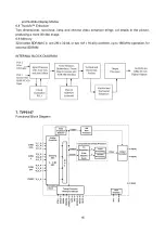
Page 13: ...11 INTERNAL BLOCK DIAGRAM...
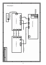
Page 26: ...Power board...
Page 27: ...Power board power board...
Page 39: ...APPENDIX Exploded view PH 42X6...
Page 42: ...603 PH42R60 10 Ver 1 0...


