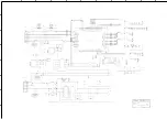
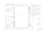
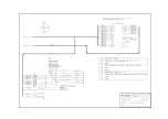
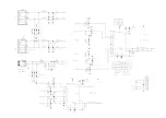

1.0
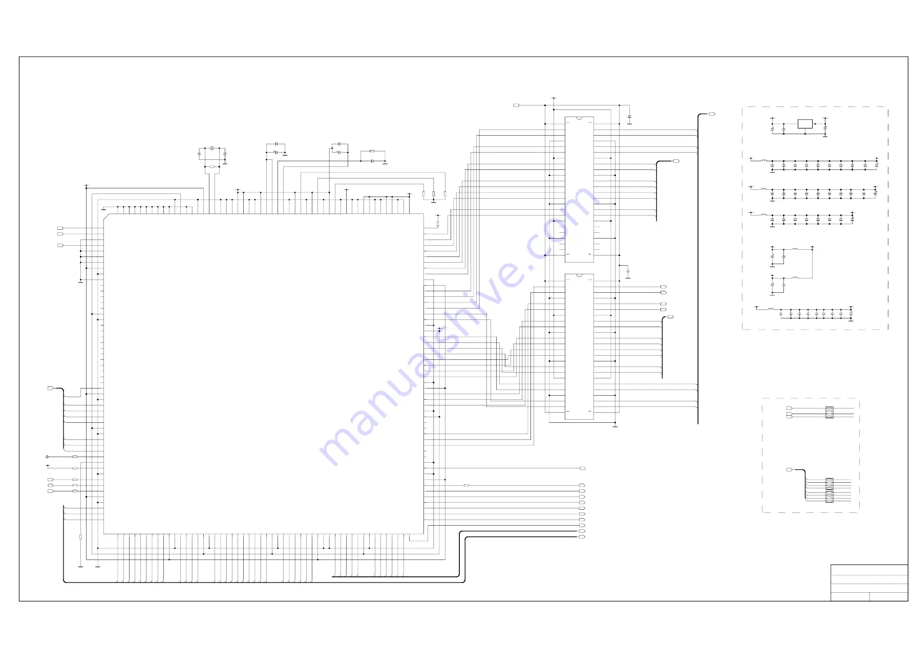
CPU
203-L37R70-01DL
XOCECO
XIAMEN OVERSEAS CHINESE
ELECTRONIC CO., LTD.
TITLE:
DWG NO.
REV.
Sheet 3 of 7
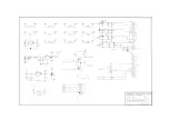
FLIBO[0]
DEC_VS
SW_SDA
23SDD[16]
23SDA[1]
FLIBO[7]
DEC_CLK
DEC_Y[0]
VRED[7]
/RESET
23SDD[17]
23SDA[0]
FLIBO[5]
23SDD[18]
FLIBO[4]
DACRST#
VGRN[1]
23SDWE#
RDACOUT
23SDD[19]
FLIBO[3]
VCLK
23SDD[20]
FLIBO[2]
GDACOUT
VGRN[3]
23SDD[21]
FLIBO[6]
BDACOUT
23SDD[22]
DEC_Y[7]
VBLU[7-0]
23SDD[23]
DEC_Y[6]
23SDD[24]
DEC_Y[5]
23SDD[25]
DEC_Y[4]
VRED[7-0]
23SDD[26]
DEC_Y[3]
23SDD[27]
DEC_Y[2]
23SDD[31-0]
VGRN[7-0]
23SDD[28]
23SDCLKI
DEC_Y[1]
23SDD[2]
23SDD[29]
SDCKO
DEC_Y[0]
23SDD[1]
23SDD[30]
DEC_Y[7-0]
23SDD[0]
23SDRAS#
23SDD[31]
23SDD[3]
23SDCAS#
VBLU[2]
23SDD[4]
23SDBA1
VBLU[3]
23SDD[5]
23SDBA0
23SDD[6]
23SDA[10-0]
23SDCS#
23SDD[7]
23SDA[10]
23SDDQM
23SDD[8]
23SDA[9]
VBLU[7]
23SDD[9]
DEC_Y[7]
23SDA[8]
23SDD[10]
DEC_Y[6]
23SDA[7]
23SDD[11]
DEC_Y[5]
23SDA[6]
FLIHS
23SDD[12]
DEC_Y[4]
23SDA[5]
FLIVS
23SDD[13]
DEC_Y[3]
23SDA[4]
FLICLK
23SDD[14]
DEC_Y[2]
23SDA[3]
FLIBO[1]
DEC_HS
VRED[5]
SW_SCL
23SDD[15]
DEC_Y[1]
23SDA[2]
2300OE#
FLIGO[5]
FLIGO[4]
FLIGO[3]
FLIGO[2]
FLIGO[1]
FLIGO[0]
FLIRO[7]
FLIRO[6]
VGRN[6]
VGRN[5]
VGRN[4]
VRED[6]
VBLU[0]
VBLU[1]
SHREF
VVS
VHS
FLIGO[7]
FLIRO[4]
FLIRO[5]
VGRN[7]
VRED[4]
VGRN[0]
FLIGO[6]
VGRN[2]
FLIHS
FLIVS
FLIRREF
FLICLK
FLIBO[0]
FLIBO[1]
FLIBO[2]
FLIBO[3]
FLIBO[4]
FLIBO[5]
FLIBO[6]
FLIBO[7]
FLIRO[0]
FLIRO[1]
FLIRO[2]
FLIRO[3]
VBLU[4]
VBLU[5]
VBLU[6]
VRED[0]
VRED[1]
VRED[2]
VRED[3]
BUFFER_OE
SW_SCL
C87
100n
DEC_VS
VRED[7-0]
3V3SC
C104
22uF
10V
R78
100
23SDDQM
L21
STBL3216-601
C111
100n
C88
100n
23SDWE#
C75
100n
C109
22uF
10V
L19
STPB3216-380PT
R93
75/1%
R84
470K
+1.8V_SW
DAC3.3V
C92
100n
1
HSYNC1_PORT1
2
VSYNC1_PORT1
3
FIELD ID1 PORT1
4
IN_CLK1_PORT1
5
HSYNC2_PORT1
6
VSYNC2_PORT1
7
FIELD ID2_PORT1
8
VDD1(3.3)
9
VSSio
10
IN_CLK2_PORT1
11
B/Cb/D1_0
12
B/Cb/D1_1
13
B/Cb/D1_2
14
B/Cb/D1_3
15
B/Cb/D1_4
16
VDDcore1(1.8)
17
VSScore
18
B/Cb/D1_5
19
B/Cb/D1_6
20
B/Cb/D1_7
26
R/Cr/CbCr_5
27
R/Cr/CbCr_6
28
R/Cr/CbCr_7
29
G/Y/Y_0
30
VDD2(3.3)
31
VSSio
32
G/Y/Y_1
33
G/Y/Y_2
34
G/Y/Y_3
35
G/Y/Y_4
36
VDDcore2(1.8)
37
VSScore
38
G/Y/Y_5
39
G/Y/Y_6
40
G/Y/Y_7
41
IN_SEL
42
TEST
43
DEV_ADDR1
44
DEV_ADDR0
45
SCLK
56
SDRAM D6
57
SDRAM D7
58
SDRAM D8
59
SDRAM D9
60
SDRAM D10
61
SDRAM D11
62
VDD4(3.3)
63
VSSio
64
SDRAM D12
65
SDRAM D13
66
SDRAM D14
67
SDRAM D15
68
VDDcore3(1.8)
69
VSScore
70
SDRAM D16
71
SDRAM D17
72
SDRAM D18
73
SDRAM D19
74
SDRAM D20
75
SDRAM D21
81
VSScore
82
SDRAM D26
83
SDRAM D27
84
SDRAM D28
85
SDRAM D29
86
SDRAM D30
87
SDRAM D31
88
VDD5(3.3)
89
VSSio
90
TEST IN
91
SDRAM ADDR10
92
SDRAM ADDR9
93
SDRAM ADDR8
94
SDRAM ADDR7
95
SDRAM ADDR6
96
VDDcore5(1.8)
97
VSScore
98
SDRAM ADDR5
99
SDRAM ADDR4
100
SDRAM ADDR3
21
R/Cr/CbCr_0
22
R/Cr/CbCr_1
46
SDATA
47
REST_N
54
SDRAM D4
55
SDRAM D5
79
SDRAM D25
80
VDDcore4(1.8)
23
R/Cr/CbCr_2
24
R/Cr/CbCr_3
25
R/Cr/CbCr_4
48
VDD3(3.3)
49
VSSio
50
SDRAM D0
51
SDRAM D1
52
SDRAM D2
53
SDRAM D3
76
SDRAM D22
77
SDRAM D23
78
SDRAM D24
101
SDRAM ADDR2
102
SDRAM ADDR1
103
SDRAM ADDR0
104
SDRAM WEN
105
SDRAM RASN
106
SDRAM CASN
107
SDRAM BA1
108
SDRAM BA0
109
SDRAM CSN
110
SDRAM DQM
111
SDRAM CLKOUT
112
VDD6(3.3)
113
VSSio
114
SDRAM CLKIN
115
TEST3
116
TEST OUT0
117
TEST OUT1
118
CTLOUT0
119
CTLOUT1
120
CTLOUT2
121
CTLOUT3
122
CTLOUT4
123
VDDcore6(1.8)
124
VSScore
125
CLKOUT
126
B/U/b_OUT_0
127
B/U/b_OUT_1
128
VDD7(3.3)
129
VSSio
130
B/U/b_OUT_2
131
B/U/b_OUT_3
132
B/U/b_OUT_4
133
B/U/b_OUT_5
134
B/U/b_OUT_6
135
B/U/b_OUT_7
136
R/Y/Pr_OUT_0
137
R/Y/Pr_OUT_1
138
VDDcore7(1.8)
139
VSScore
140
R/Y/Pr_OUT_2
141
R/Y/Pr_OUT_3
142
R/Y/Pr_OUT_4
143
R/Y/Pr_OUT_5
144
R/Y/Pr_OUT_6
145
R/Y/Pr_OUT_7
146
VDD8(3.3)
147
VSSio
148
G/Y/Y_OUT_0
149
G/Y/Y_OUT_1
150
G/Y/Y_OUT_2
151
G/Y/Y_OUT_3
152
G/Y/Y_OUT_4
153
G/Y/Y_OUT_5
154
G/Y/Y_OUT_6
155
G/Y/Y_OUT_7
156
OE
157
PLL_PVDD(1.8)
158
PLL_PVSS
159
AVSS_PLL_BE1
160
AVDD_PLL_BE1(1.8)
161
AVDD_PLL_BE2(1.8)
162
AVSS_PLL_BE2
163
AVSS_PLL_SDI
164
AVDD_PLL_SDI(1.8)
165
AVDD_PLL_FE(1.8)
166
AVSS_PLL_FE
167
DAC_PVSS
168
DAC_VDD(1.8)
169
DAC_VSS
170
DAC_BOUT
171
DAC_AVDDB(3.3)
172
DAC_AVSSB
173
DAC_GOUT
174
DAC_AVDDG(3.3)
175
DAC_AVSSG
176
DAC_ROUT
177
DAC_AVDDR(3.3)
178
DAC_AVSSR
179
DAC_COMP
180
DAC_REST
181
DAC_VREFOUT
182
DAC_VREFIN
183
DAC_AVDD(3.3)
184
DAC_AVSS
185
DAC_GR_AVSS
186
DAC_GR_AVDD(3.3)
187
DAC_PVDD(3.3)
188
TEST0
189
TEST1
190
TEST2
191
XTAL IN
192
XTAL OUT
193
VDD9(3.3)
194
VSSio
195
IN_CLK_PORT2
196
D1_IN_0
197
VDDcore(1.8)
198
VSScore
199
D1_IN_1
200
D1_IN_2
201
D1_IN_3
202
D1_IN_4
203
D1_IN_5
204
D1_IN_6
205
D1_IN_7
206
FID_PORT2
207
VS_PORT2
208
HS_PORT2
C105
22uF
10V
G3
13.5MHz
R82
10K
VVS
3.3VS23
C81
100n
23SDCAS#
C95
100n
C96
100n
3V3SC
C103
100n
C85
100n
C79
100n
PLL1.8V
C84
100n
DEC_CLK
VBLU[7-0]
R81
100
N11
AS1117-1V8
IN
OUT
23SDCS#
R95
100
+1.8V_SW
C102
100n
C112
100n
PLL1.8V
23SDA[10-0]
C82
47uF
10V
C94
100n
R90
0
C108
22uF
10V
C89
100n
L23
STBL3216-601
R91
75/1%
C90
33p
C99
100n
R88
0
TP3
C113
22uF
10V
VHS
DAC1.8V
C106
100n
C97
100n
23SDRAS#
C74
100n
C93
100n
3V3SC
1.8VS23
3.3VS23
C77
100n
/RESET
VCLK
DEC_Y[7-0]
23SDBA0
R80
100
R92
10K
C73
100n
23SDD[31-0]
3V3SC
C101
47uF
10V
C80
100n
C83
100n
C100
22uF
10V
DEC_HS
L20
STPB3216-380PT
VGRN[7-0]
DAC1.8V
1.8VS23
23SDCLKI
C107
22uF
10V
C78
100n
L22
STBL3216-601
C110
100n
R94
75/1%
C98
33p
23SDCLKI
R89
0
C114
100n
C76
100n
+1.8V_SW
C86
100n
R83
22
DEC_Y[7-0]
SHREF
R85
180
23SDBA1
DAC3.3V
3.3VS23
C91
100n
R79
100
SW_SDA
DEC_CLK
DEC_VS
DEC_HS
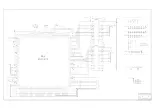
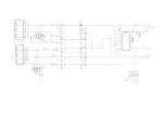
N35
74LV16244MTD
38
I6
1
OE1
11
O6
47
Io
3
O1
8
O4
6
O3
46
I1
39
GND39
45
GND45
7
Vcc7
5
O2
42
Vcc42
9
O5
40
I5
10
GND10
41
I4
4
GND4
43
I3
48
OE2
2
Oo
44
I2
12
O7
37
I7
13
O8
14
O9
35
I9
36
I8
15
GND15
34
GND34
16
O10
33
I10
17
O11
18
Vcc18
31
Vcc31
32
I11
19
O12
20
O13
29
I13
30
I12
21
GND21
28
GND28
22
O14
23
O15
24
OE4
25
OE3
26
I15
27
I14
N36
74LV16244MTD
38
I6
1
OE1
11
O6
47
Io
3
O1
8
O4
6
O3
46
I1
39
GND39
45
GND45
7
Vcc7
5
O2
42
Vcc42
9
O5
40
I5
10
GND10
41
I4
4
GND4
43
I3
48
OE2
2
Oo
44
I2
12
O7
37
I7
13
O8
14
O9
35
I9
36
I8
15
GND15
34
GND34
16
O10
33
I10
17
O11
18
Vcc18
31
Vcc31
32
I11
19
O12
20
O13
29
I13
30
I12
21
GND21
28
GND28
22
O14
23
O15
24
OE4
25
OE3
26
I15
27
I14
BUFFER_OE
L55
STBL3216-601
C322
22uF
10V
C323
100n
C324
100n
C325
100n
C326
100n
C327
100n
C328
100n
C329
100n
C330
100n
C331
100n
C332
100n
3V3SC
BUF3.3V
BUF3.3V
N10
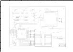
FLI2310
4
4
4
4
I2C ADDRESS=0XD2
4
4
1,5
1,5
4
1,5
4
4
4
4
DEINTERLACER
2
2
2
2
1,5
5
1,5
1,5
2
2
2
2
2
2
2,5
DECOUPLING FOR FLI2310
I 1.8VS23<=550mA
I 3.3VS23<=225mA
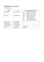
Summary of Contents for PH-42R6
Page 1: ...PDP TELEVISION PH 42R6 Canada...
Page 11: ...9 Fig 1 1 Simplified functional block diagram of the MSP 34x0G...
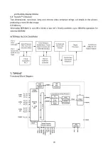
Page 13: ...11 INTERNAL BLOCK DIAGRAM...
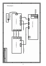
Page 26: ...Power board...
Page 27: ...Power board power board...
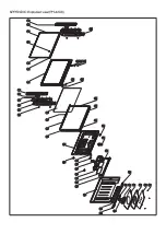
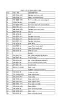
Page 39: ...APPENDIX Exploded view PH 42X6...
Page 42: ...603 PH42R60 10 Ver 1 0...


