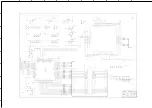
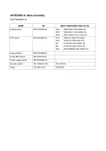

1.0
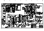
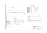
CPU
203-L37R70-01DL
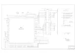
Place this parallel termination close to
corresponding memory IC pins
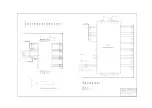
XOCECO
XIAMEN OVERSEAS CHINESE
ELECTRONIC CO., LTD.
TITLE:
DWG NO.
REV.
Sheet 4 of 7
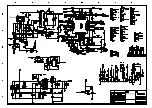
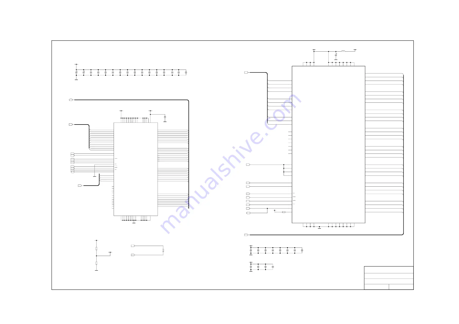
Frame Memory
23SDD[31-0]
23SDA[10-0]
23SDD[0]
23SDD[1]
23SDD[2]
23SDD[3]
23SDD[4]
23SDD[5]
23SDD[6]
23SDD[7]
23SDD[8]
23SDD[9]
23SDD[10]
23SDD[11]
23SDD[12]
23SDD[13]
23SDD[14]
23SDD[15]
23SDD[16]
23SDD[17]
23SDD[18]
23SDD[19]
23SDD[20]
23SDD[21]
23SDD[22]
23SDD[23]
23SDD[24]
23SDD[25]
23SDD[26]
23SDD[27]
23SDD[28]
23SDD[29]
23SDD[30]
23SDD[31]
23SDA[0]
23SDA[1]
23SDA[2]
23SDA[3]
23SDA[4]
23SDA[5]
23SDA[6]
23SDA[7]
23SDA[8]
23SDA[9]
23SDA[10]
23SDDQM
23SDBA0
23SDBA1
23SDWE#
23SDCAS#
23SDRAS#
23SDCS#
FSVREF
FSCLK+
FSCLK-
FSADDR[0-11]
FSDATA[0-31]
FSADDR[0]
FSADDR[1]
FSADDR[2]
FSADDR[3]
FSADDR[4]
FSADDR[5]
FSADDR[6]
FSADDR[7]
FSADDR[8]
FSADDR[9]
FSADDR[10]
FSADDR[11]
FSDATA[0]
FSDATA[1]
FSDATA[2]
FSDATA[3]
FSDATA[4]
FSDATA[5]
FSDATA[6]
FSDATA[7]
FSDATA[8]
FSDATA[9]
FSDATA[10]
FSDATA[11]
FSDATA[12]
FSDATA[13]
FSDATA[14]
FSDATA[15]
FSDATA[16]
FSDATA[17]
FSDATA[18]
FSDATA[19]
FSDATA[20]
FSDATA[21]
FSDATA[22]
FSDATA[23]
FSDATA[24]
FSDATA[25]
FSDATA[26]
FSDATA[27]
FSDATA[28]
FSDATA[29]
FSDATA[30]
FSDATA[31]
FSDQM[0]
FSDQM[1]
FSDQM[2]
FSDQM[3]
FSBKSEL0
FSBKSEL1
FSDQM[0-3]
FSCLK-
FSCLK+
FSCKE
/FSRAS
/FSCAS
/FSWE
FSDQS
23SDCLKI
80
DQ12
1
VDD1
11
DQ6
3
VDDQ3
8
DQ4
6
VSSQ6
81
VDDQ81
7
DQ3
5
DQ2
84
VSSQ84
9
VDDQ9
10
DQ5
83
DQ14
4
DQ1
85
DQ15
2
DQ0
86
VSS86
12
VSSQ12
79
DQ11
13
DQ7
77
DQ10
78
VSSQ78
15
VDD15
76
DQ9
16
DQM0
75
VDDQ75
17
WE
18
CAS
74
DQ8
19
RAS
20
CS
71
DQM1
72
VSS72
22
BA0
23
BA1
24
A10
67
CKE
68
CLK
25
A0
26
A1
27
A2
28
DQM2
63
A6
64
A7
65
A8
66
A9
29
VDD29
32
VSSQ32
59
DQM3
60
A3
61
A4
62
A5
33
DQ17
34
DQ18
35
VDDQ35
36
DQ19
37
DQ20
38
VSSQ38
39
DQ21
40
DQ22
41
41
42
DQ23
43
VDD43
44
VSS44
58
VSS58
56
DQ31
55
VDDQ55
54
DQ30
53
DQ29
52
VSSQ52
51
DQ28
50
DQ27
49
VDDQ49
48
DQ26
47
DQ25
46
VSSQ46
45
DQ24
82
DQ13
31
DQ16
14
NC14
21
NC21
30
NC30
57
NC57
69
NC69
70
NC70
73
NC73
23SDDQM
23SDBA0
23SDBA1
23SDWE#
23SDCAS#
23SDRAS#
23SDCS#
23SDCLKI
23SDD[31-0]
R106
1K
23SDA[10-0]
L24
STPB3216-380PT
R103
10K
R104
10K
R105
137
FSCLK+
FSCLK-
N12
MT46V2M32LG
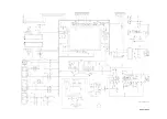
14
VDDQ
5
VSSQ
2
VDDQ
8
VDDQ
50
A7
49
A6
48
A5
47
A4
34
A3
33
A2
32
A1
31
A0
22
VDDQ
27
RAS
11
VSSQ
59
VDDQ
19
VSSQ
53
CKE
28
CS
13
DQ19
VDDQ
67
62
VSSQ
35
VDD
76
VSSQ
64
DQ11
63
DQ10
61
DQ9
60
DQ8
VDDQ
79
66
VSS
82
VSSQ
7
DQ7
6
DQ6
4
DQ5
3
DQ4
VDDQ
86
1
DQ3
100
DQ2
98
DQ1
97
DQ0
92
VSSQ
99
VSSQ
65
VDD
15
VDD
16
VSS
12
DQ18
69
DQ13
68
DQ12
46
VSS
10
DQ17
9
DQ16
70
VSSQ
VDDQ
73
72
DQ15
71
DQ14
VDDQ
95
54
CLK
29
BA0
36
A10
51
A8/AP
37
A11
45
A9
55
CLK
30
BA1
96
VDD
58
VREF
85
VSS
52
MCL
94
DQS
25
WE
26
CAS
57
DM3
24
DM2
56
DM1
23
DM0
41
NC
40
NC
39
NC
38
NC
42
NC
88
NC
87
NC
44
NC
43
NC
89
NC
90
NC
91
NC
93
NC
17
DQ20
18
DQ21
20
DQ22
21
DQ23
74
DQ24
75
DQ25
77
DQ26
78
DQ27
80
DQ28
81
DQ29
83
DQ30
84
DQ31
FSDATA[0-31]
FSADDR[0-11]
FSDQM[0-3]
FSBKSEL0
FSBKSEL1
FSCLK-
FSCLK+
FSCKE
/FSRAS
/FSCAS
/FSWE
FSDQS
23SDCLKI
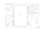
C134
100n
C139
100n
C118
100n
C125
100n
C136
100n
C133
100n
C119
100n
C126
100n
C138
100n
C135
100n
C120
100n
C127
100n
C140
100n
C137
100n
C121
100n
C129
100n
C141
100n
C122
100n
C130
100n
C142
100n
C123
100n
C131
100n
C132
100n
C128
100n
C143
100n
C117
100n
C124
100n
C115
22uF
10V
C116
22uF
10V
+2.5V_DDR
+2.5V_DDR
FSVREF
+2.5V_DDR
FSVREF
3.3VSDRAM1
3.3VSDRAM1
3.3VSDRAM1
3.3VSDRAM1
3V3SC
C144
47uF
10V
3
3
3
3
3
3
3
3
3
3
3
5
5
5
5
5
5
5
5
5
5
5
5
N13
MT48LC2M32B2TG
Summary of Contents for PH-42R6
Page 1: ...PDP TELEVISION PH 42R6 Canada...
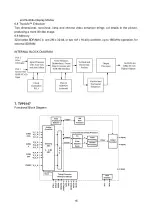
Page 11: ...9 Fig 1 1 Simplified functional block diagram of the MSP 34x0G...
Page 13: ...11 INTERNAL BLOCK DIAGRAM...
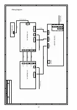
Page 26: ...Power board...
Page 27: ...Power board power board...
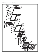
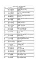
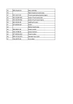
Page 39: ...APPENDIX Exploded view PH 42X6...
Page 42: ...603 PH42R60 10 Ver 1 0...


