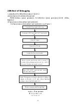
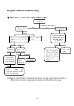
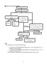
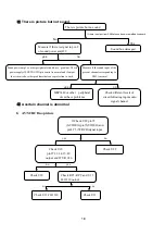
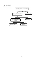
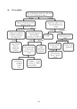
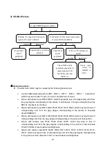
background image

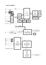
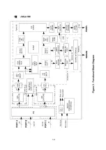
and then it is also sent to U13 in YUV format of 24bit. 

24bit RGB signal is output and sent to main processing IC JAG-ASM(U12) after the 

above two routes of signal are processed in matrix , color density, and tint in U13.. Another 
route of RGB signal of computer VGA is also sent to U12, where two routes of signal are 
subject to selection and processing for picture format. One route RGB signal of VGA 
undergoes A/D conversion before being subject to selection and digit display processing 
together with another route of signal, including OSD, GAMMA calibration, brightness and 
contrast processing. These signals are changed into the format of 1024*768. The above 
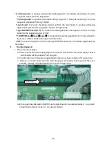
RGB signal of 24 bit is output to LVDS converter DS90C385(U31)of; where it is converted 
into four pairs of low voltage differential signal acceptable for PDP screen. Then, the signal 
is sent to PDP screen for picture display. 

The audio R/L of left and right sound channels D4,YCbCr and BS undergoes selection 

and is then sent to MSP3420(NA04). AV,SVHS and R/L of VGA are sent to NAQ04.In NA04, 
the second sound IF( SIF) is demodulated into audio signal together with other four routes 
of sound signal being switched for selection. The selected R/L after the processing in 
volume and sound effect is then output. One route MONO sound is for AV OUT, the other 
route is sent to M62494(NA08)of SRS sound field processor for SRS processing. The 
signal, after sound power amplification by TPA3001(NA10,NA11), is for driving the speaker. 
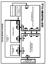
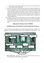
BS tuner outputs other route BIT/DET. The power is supplied by power supply board on 
PDP screen and then transformed into different required power supplies.   


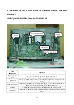
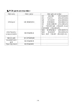
Summary of Contents for PS42K8

Page 1: ...COLOR TELEVISION PS42K8...

Page 2: ...higher than the specification If the power supply used deviates from the value given in the specification there might be a possibility of leading to fire or damage to the module 4 Never have operatio...

Page 3: ...ope for operation 0 50centigrade Scope for storage 15 60centigrade Humidity Scope for operation 20 80 Scope for storage 20 80 15 If a fixed picture is displayed for a long time difference in its brigh...

Page 4: ...for Identifying the Defects on Screen The PDP produced by our Company at present uses the following criterion for identifying the defective points 2 1 Model PS 42D8 There may appear three kinds of de...

Page 5: ...d and AV or TV board on the line Check CPU board Check AV or TV board Combined test for general assembly Connect to central signal source check if various TV functions station skipping analog control...

Page 6: ...justment of VGA channel Adjust ADC gain to 15 5 2 3 White balance adjustment of VGA channel Input K 7253 TIME303 640 480 60Hz PATTERN471 and the signal of 8 grades of grey density Enter the adjustment...

Page 7: ...TIME380 480i PATTERN471 adjust s bright to 120 S contrast to 130 Enter the adjustment menu of white balance adjust second grade with balancer Adjust offset_R offset_G offset_B so that the second grad...

Page 8: ...ogies The working principal is similar to normal fluorescent lamp The color picture of the TV is formed of the light emissions by each pixel unit of fluorescent powder Thus the picture looks bright fr...

Page 9: ...U31 of where it is converted into four pairs of low voltage differential signal acceptable for PDP screen Then the signal is sent to PDP screen for picture display The audio R L of left and right soun...

Page 10: ...V OUT U30 ADC MST9883 U3 EEPROM U2 MICRO CONTRLER TSC80251G2D U4 FLASHMEMORY IR SIF S VGA AV MONO OUT NA04 AUDIO PROCESSOR MSP3420 NA08 SRS 3D STEREO CONTROLLER M62494 2 BLOCK DIAGRAM I C BUS 2 24bit...

Page 11: ...10 4 IC BLOCK 1 MSP3420...

Page 12: ...11 2 VPC3230...

Page 13: ...12 3 JAG ASM...

Page 14: ...PS42K8 WIRING DIAGRAM 335 42001 00 PANEL LOGIC CIRCUIT BOARD POWER BOARD SOUND BOX PART POWER FILTER BOARD 667 PS42K8 40 ADUIO VIDEO PROCESSOR BOARD 667 MS42K8 56 CPU BOARD 667 PS42K8 05 KEYSETS...

Page 15: ...from the processing board into the one displayable by screen Addressing circuit Addressing circuit for screen display directly driving the address electrode on the screen Vertical electrode totally 8...

Page 16: ...0D 353 32300 80 U30 MST9883B 353 98830 10 U31 DS90C385MTD 353 03850 20 U2 TSC80251G2D 353 80251 10 U4 AT49F002NT 352 49002 70 video frequency processor boards 667 PS42K8 40 NA04 MSP3420G Q 353 34200 1...

Page 17: ...ion functions If there is over current or over voltage this protection will function and no output Three no check5V STBY Cutoff the connection between power board and signal process check5V STB Cutoff...

Page 18: ...sure resume it to the original status when the check is over With sound but no picture If there is interface for switch on Check if no image for all other channels N501 and peripheral Change into 4 ch...

Page 19: ...ormal and if output short circuited or other problems that cause protection to work Measure if there is signal in pin 2 of sound power amplf 2 Measure if the sound input of the present channel corresp...

Page 20: ...19 2 D4 no picture yes no yes no yes Check U30 pin48 Y and pin49 SOG Check D4 to U30 Check RP36 RP41 RP141 and U30 Check RP3 RP9 and U13 FLI2310 Check U30 Check U13 FLI2310 Check U12...

Page 21: ...tput circuit Check output signal of N102 line field synchronous clk PEN etc N204 and its peripheral circuits have Peripheral circuits of N501 V PORT have problem Input an AV signal to see if the AV of...

Page 22: ...loss of corresponding color from the gray degree corresponding to the picture of channel DVI Failure with resistor rows R342 R343 R344 R345 which may lead to loss of corresponding color from the gray...

Page 23: ...k as explained above No brightness in the square block area Normally it s caused by the damage of the address BUFFER module that directly corresponds to its position or may be caused by the damage of...

Page 24: ...mit the scanning signal from the Y driving board to the screen which is divided into upper and lower parts COF to convert the signal sent from the logic BUFFER board into the address signal used by th...

Page 25: ...appears on the screen a line or several unlit lines Check if the socket between Y driving board and Y BUFFER is plugged well If not plug it well If yes then replace Y BUFFER upper lower in respect to...

Page 26: ...OF or the screen b If it s an entire vertical block of other colors then first check to see if the connection socket between COF and logice BUFFER has problem If no problem check if the connection soc...

Page 27: ......

Page 28: ......

Page 29: ......

Page 30: ......

Page 31: ......

Page 32: ......

Page 33: ......

Page 34: ......

Page 35: ......

Page 36: ......

Page 37: ......

Page 38: ......

Page 39: ......

Page 40: ......

Page 41: ......

Reviews: