background image

7

FT-250R Technical Supplement

Circuit Description

Receive Signal Path

Incoming RF from the antenna jack is delivered to the RF
Unit and passes through a low-pass filter and high-pass
filter consisting of coils L1001, L1002, L1003, L1004, L1014
& L1015, capacitors C1001, C1002, C1003, C1004, C1006,
C1007, C1042, C1044, C1045, C1046 & C1047, and anten-
na switching diode 

D1001

 (

RLS135

).

Signals within the frequency range of the transceiver are
then amplified by 

Q1011

 (

2SC5006

) and enter a varac-

tor-tuned band-pass filter consisting of coils L1016, L1017
& L1018, capacitors C1049, C1050, C1051, C1052, C1053,
C1054, C1056, C1057, C1058, C1059, C1060, C1061, C1062
& C1063, and diodes 

D1004

D1005

 & 

D1006

 (all

HVC350B

) before delivery to the first mixer, 

Q1013

(

3SK296ZQ

).

Buffered output from the VCO is amplified by 

Q1018

(

2SC5374

) to provide a pure first local signal between

122.3 and 126.3 MHz according to the transceiver version
and the programmed receiving frequency for injection to
the first mixer Q1013. The 21.7 MHz first mixer product
then passes through monolithic crystal filter XF1001
(21R12A4, 6 kHz BW) to strip away unwanted mixer prod-
ucts, and the IF signal is then amplified by 

Q1014

(

2SC4400

).

The amplified first IF signal is applied to FM IF subsystem
IC 

Q1017

 (

TA31136FN

), which contains the second mix-

er, limiter amplifier, noise amplifier, and S-meter ampli-
fier.

A second local signal is generated by the reference oscil-
lator section of the PLL subsystem IC 

Q1030

(

MB15A01PFV1

) using 21.25 MHz crystal X1001; a 450

kHz second IF is produced when this signal is mixed with
the first IF signal within Q1017.

The second IF then passes through the main selectivity
element, ceramic filter 

CF1001

 (

CFWM450E

) to strip away

all but the desired signal; it is then applied to the limiter
amplifier in Q1017, which removes amplitude variations
in the 450kHz IF, before detection of the speech by the
ceramic discriminator 

CD1001

 (

JTBM450CX24

).

Detected audio from Q1017 is applied to a low-pass filter
consisting of capacitors C1208, C1209 & C1210, resistors
R1320, R1321, R1322, R1323 & R1324, and 

Q1060

(

NJM2902V

), then passes through the audio mute gate

Q1044

 and 

Q1063

 (both 

2SC4081

) to the buffer amplifi-

er 

Q1043

 (

2SC4617

); it is then passed through the de-

emphasis network consisting of capacitor C1057 and re-
sistor R1208 to a high-pass filter consisting of capacitors
C1058, C1059 & C1060, resistors R1209 & R1210, and

Q1064

 (

NJM2902V

).

The processed audio passes through the another audio
mute gate 

Q1041

 and 

Q1042

 (both 

2SC4081

) to the vol-

ume control potentiometer VR3001 on the VR Unit, then
is delivered to the audio amplifier 

Q1053

 (

DTA2822L

),

which provides up to 0.5 Watt to the headphone jack or
an 8-W loudspeaker.

Squelch Control

The squelch circuitry consists of a noise amplifier, band-
pass filter, noise detector & noise comparator within

Q1017

, audio control gate 

Q1041

Q1042

Q1044

Q1063

(all 

2SC4081

), microprocessor 

Q1035

 (

M3826AEFGP

),

and squelch controller S3001 on the VR Unit.

When no carrier received, noise at the output of the de-
tector stage in Q1017 is amplified and band-pass filtered
by the noise amplifier section of Q1017 and the network
between pins 7 and 8, and then rectified by the noise de-
tector section of Q1017. The resulting DC squelch control
voltage outputs at pin 13 of Q1017, then it is passed to pin
4 of the microprocessor Q1035.

If no carrier is received, this signal causes pins 44 and 47
of Q1035 to go “Low” and pin 54 to go “High.” Pin 47
disables the supply voltage to the audio amplifier 

Q1053

(

TDA2822L

), and pin 54 activates the audio control gates

Q1041, Q1042, Q1044, Q1063, Q1049 and Q1050. Thus, the
microprocessor Q1035 blocks output from the audio am-
plifier, and silences the receiver, while no signal is being
received (and during transmission, as well). Meanwhile,
pin 44 signals 

Q1056

 (

2SC4081

) to hold the green (Busy)

half of the LED 

D3001

 (

BRPY1211F

) on the VR Unit off.

When a carrier appears at the discriminator, noise is re-
moved from the output, causing pin 4 of Q1035 to go “low”
and the microprocessor to activate the audio amplifier,
audio mute gate, and “Busy” LED.

The microprocessor then checks for CTCSS or CDCSS code
squelch information, if enabled, or for DTMF data on the
optional DTMF Unit. If not transmitting and CTCSS or
CDCSS is not activated, or if the received tone or code
matches that programmed, the microprocessor stops scan-
ning (if active) and allows audio to pass through the au-
dio amplifier Q1053 to the loudspeaker by enabling the
supply voltage to it via 

Q1047

 (

2SB1132Q

), 

Q1048

(

UMW1

).

Summary of Contents for FT-250R

Page 1: ...rs ICs etc or leaded components only While we believe the information in this manual to be correct VERTEX STANDARD assumes no liability for damage that may occur as a result of typographical or other...

Page 2: ...x 108 5 x 26 5 mm w o knob antenna Weight approx 11 5 Oz 325g w FNB 83 Antenna and BeltClip RECEIVER Circuit type Double conversion superheterodyne Intermediate Frequency 1st 21 7 MHz 2nd 450 kHz Sens...

Page 3: ...RA0210600 RUBBER PACKING RA1111800 WINDOW RA1111900 VOLUME KNOB RA1112000 ENCODER KNOB RA0210300 RUBBER KNOB RA0211100 INTER CONNECTOR RA0211200 INTER CONNECTOR G6090137 LCD RA010690A TERMINAL PLATE L...

Page 4: ...4 FT 250R Technical Supplement Exploded View Miscellaneous Parts Note...

Page 5: ...5 Block Diagram FT 250R Technical Supplement...

Page 6: ...6 Block Diagram FT 250R Technical Supplement Note...

Page 7: ...the buffer amplifi er Q1043 2SC4617 it is then passed through the de emphasis network consisting of capacitor C1057 and re sistor R1208 to a high pass filter consisting of capacitors C1058 C1059 C106...

Page 8: ...emains Low disabling the gate voltages of driv er amplifier Q1009 2SK3074 and final amplifier Q1008 RD07MVS1A thereby disabling the transmitter Spurious Suppression Generation of spurious products by...

Page 9: ...quency is at the actual transmit frequency rather than offset for IFs as in the receiving case Also the VCO is modulated by the speech audio applied to D1010 HSC277 as described previously Receive and...

Page 10: ...gnment determined to be abso lutely necessary Required Test Equipment The following test equipment and familiarity with its use is necessary for complete realignment Correction of prob lems caused by...

Page 11: ...he antenna jack select 146 MHz key the transmitter and adjust TC1001 on the Main Unit if necessary so the counter frequency is within 100 Hz of 146 MHz TX SECTION ALIGNMENT SETUP RX SECTION ALIGNMENT...

Page 12: ...l Alignment System Startup Procedure To begin set the transceiver to the 146 0000 MHz and turn the transceiver off Next press and hold in the PTT MONI and the LAMP switches hold them in while turning...

Page 13: ...hieve a 0 7 kHz 0 05 kHz reading narrow 0 5 kHz on the deviation meter Transmitter Total Deviation Select 146 MHz and adjust the AF generator attenua tor for 80 mV output at 1 kHz to the microphone ja...

Page 14: ...14 FT 250R Technical Supplement Alignment Note...

Page 15: ...6 V 1 2 V 1 1 V 0 V 3 2 V TONE SQL 67 0 Hz 151 4 Hz 3 1 V 156 7 Hz 250 3 Hz 0 V DCS 3 1 V Wide 0 V Narrow 0 6 V CHG OFF 7 2 V ON 6 4 V CHG OFF 7 0 V ON 5 7 V CHG OFF 7 0 V ON 0 V 7 0 V 6 8 V 6 7 V 7 0...

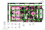
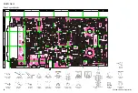
Page 16: ...16 MAIN Unit FT 250R Technical Supplement...

Page 17: ...DA221 K D1007 1017 1019 DAN222 N D1025 1026 2SB1132 BA Q1063 1078 DTA144EE 16 Q1052 2SA1774 FR Q1068 M3826AEFGP Q1035 2SC4081 Q1015 1016 1037 1038 1041 1042 1044 1056 2SC4400 Q1014 TA31136FN Q1017 2SB...

Page 18: ...8 AA1101F D1024 02CZ2 0X 2 0X D1029 2SD1664 DA Q1057 2SC4154 Q1001 1002 1006 1007 1025 1031 1034 1036 1040 1055 1059 1061 1063 1065 2SC5006 Q1011 2SC4617 BR Q1043 2SC5226 Q1010 2SC5374 Q1018 1019 1022...

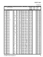
Page 19: ...82C1H330JA01D K22174223 1 B c1 C 1035 CHIP CAP 33pF 50V CH GRM1882C1H330JA01D K22174223 1 B c1 C 1036 CHIP CAP 0 001uF 50V B GRM188B11H102KA01D K22174821 1 B d1 C 1037 CHIP CAP 0 001uF 50V B GRM188B11...

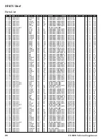
Page 20: ...HIP CAP 15pF 50V CH GRM1882C1H150JA01D K22174215 1 B d2 C 1109 CHIP CAP 18pF 50V CH GRM1882C1H180JA01D K22174217 1 B d2 C 1110 CHIP CAP 0 001uF 50V B GRM188B11H102KA01D K22174821 1 B d2 C 1111 CHIP CA...

Page 21: ...CAP 0 001uF 50V B GRM188B11H102KA01D K22174821 1 A G3 C 1190 CHIP CAP 0 001uF 50V B GRM188B11H102KA01D K22174821 1 B a4 C 1191 CHIP CAP 0 001uF 50V B GRM188B11H102KA01D K22174821 1 B b3 C 1192 CHIP CA...

Page 22: ...2070660 1 A B1 D 1022 LED AA1111C TR G2070660 1 A A3 D 1023 LED AA1111C TR G2070660 1 A B3 D 1024 LED AA1101F TR G2070658 1 B a3 D 1025 DIODE DAN222 TL G2070174 1 A C3 D 1026 DIODE DAN222 TL G2070174...

Page 23: ...G3117748R 1 B e3 Q 1033 TRANSISTOR DTA114TE TL G3070264 1 B f2 Q 1034 TRANSISTOR 2SC4081 T106 R G3340818R 1 B f1 Q 1035 IC M3826AEFGP 1 A E2 Q 1036 TRANSISTOR 2SC4081 T106 R G3340818R 1 B d3 Q 1037 TR...

Page 24: ...16W 5 RMC1 16S 473JTH J24189045 1 B c2 R 1042 CHIP RES 330 1 16W 5 RMC1 16S 331JTH J24189019 1 B c1 R 1043 CHIP RES 33 1 16W 5 RMC1 16S 330JTH J24189007 1 B d1 R 1044 CHIP RES 330 1 16W 5 RMC1 16S 331...

Page 25: ...CHIP RES 470 1 16W 5 RMC1 16S 471JTH J24189021 1 B e2 R 1114 CHIP RES 1k 1 16W 5 RMC1 16S 102JTH J24189025 1 B e2 R 1115 CHIP RES 1k 1 16W 5 RMC1 16S 102JTH J24189025 1 B e2 R 1116 CHIP RES 0 1 16W 5...

Page 26: ...1 16W 5 RMC1 16S 474JTH J24189057 1 A F1 R 1190 CHIP RES 100k 1 16W 0 5 RR0510R 104 D J24189167 1 A E2 R 1191 CHIP RES 22k 1 16W 5 RMC1 16S 223JTH J24189041 1 A D3 R 1192 CHIP RES 470k 1 16W 5 RMC1 1...

Page 27: ...65 CHIP RES 1k 1 16W 5 RMC1 16S 102JTH J24189025 1 A D2 R 1266 CHIP RES 1k 1 16W 5 RMC1 16S 102JTH J24189025 1 B c3 R 1267 CHIP RES 1k 1 16W 5 RMC1 16S 102JTH J24189025 1 A D2 R 1268 CHIP RES 1k 1 16W...

Page 28: ...JTH J24189033 1 B f3 R 1338 CHIP RES 22k 1 16W 5 RMC1 16S 223JTH J24189041 1 B f3 R 1339 CHIP RES 3 9k 1 16W 5 RMC1 16S 392JTH J24189032 1 B f3 R 1340 CHIP RES 100k 1 16W 5 RMC1 16S 104JTH J24189049 1...

Page 29: ...Unit FT 250R Technical Supplement HOLDER RA0210100 1 TERMINAL PLATE RA0210700 1 SHEET RA023330A 1 LIGHT GUIDE RA020950A 1 Parts List REF DESCRIPTION VALUE V W TOL MFR S DESIG VXSTD P N VERS LOT SIDE...

Page 30: ...30 MAIN Unit FT 250R Technical Supplement Note...

Page 31: ...uF 50V B K22174817 1 C 3002 CHIP CAP 0 0047uF 50V B K22174817 1 D 3001 LED G2070706 1 R 3001 CHIP RES 100ohm 1 16W 5 J24189013 1 S 3001 ROTARY ENCODER Q9000739 1 VR3001 POT J60800236 1 VR3001 POT J608...

Page 32: ...12 1 A R 5001 CHIP RES 18k 1 16W 5 RMC1 16 183JATP J24185183 1 A DESCRIPTION VALUE V W TOL YAESU P N MFR S DESIG VERS REF LOT SIDE SW UNIT PCB with Components CB4883001 Printed Circuit Board FR002650B...

Page 33: ...Copyright 2009 VERTEX STANDARD CO LTD All rights reserved No portion of this manual may be reproduced without the permission of VERTEX STANDARD CO LTD...

Reviews: