background image

FT-712RH

TECHNICAL SUPPLEMENT

YAESU MUSEN CO., LTD.

C.P.O. BOX 1500

TOKYO, JAPAN

MFlNURLC DI SERV. X

rr-pia RH

05910739

Summary of Contents for FT-712RH

Page 1: ...FT 712RH TECHNICAL SUPPLEMENT YAESU MUSEN CO LTD C P O BOX 1500 TOKYO JAPAN MFlNURLC DI SERV X rr pia RH 05910739...

Page 2: ...mponents and the other has either a mixture of both chip and lead components trimmers coils electrolytic capacitors packaged ICs etc or lead components only The two obverse views depict the board a it...

Page 3: ...f its bracket 2 Remove the three screws in the arms of the speaker bracket and remove the bracket TOP COVER REMOVAL Removing the top cover exposes the Solder Side of the Main Unit circuit board and th...

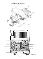
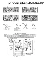
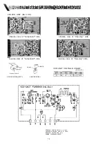
Page 4: ...PA UNIT APC UNIT 430 VCO UNIT LCD UNIT CONTROL UNIT BOARD LAYOUT 2...

Page 5: ...MAIN UNIT No 1 XXX obverse view of component side 3 SOURCE DRAIN GATE 2 Marked surface 3SK164 F 01001 3SK165 J 01002 M54959P 01013 pPC7805H 01018 L7809 01017 TDA2003 01008...

Page 6: ...ITTER COLLECTOR BASE 2SB1134R Q1016 COLLECTOR EMITTER BASE 2S02407 A Q1010 BASE COLLECTOR EMITTER 2SD1000 LL Of007 2SC3357 RK 01009 GATE Marked Surface 2SK208Y JY 01014 reverse view of component side...

Page 7: ...d surface 2SA812 M7 01005 2SC1623 I_7 01004 1006 1015 2SC2620 QB 01003 2SC3356 R24 0 1 0 1 1 1 0 1 2 Marked Surface 1SS184 B3 D1001 HSM2693 B2 D1005 ANODE l CATHODE 2 1SS226 C3 D1002 obverse view of c...

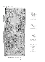
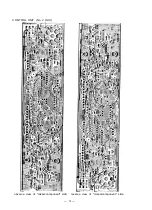
Page 8: ...reverse view of chip only side 6...

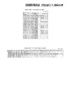
Page 9: ...MAIN UNIT VOLTAGE CHART DC VOLTS MAIN UNIT 1C VOLTAGE CHART DC VOLTS...

Page 10: ...chip only side reverse view of mixed component side reverse viewof chip only side Marked Surface M5223FP Q403 2SC1623 L6 Q402 TK10487M Q401 IF UNIT VOLTAGE CHART DC VOLTS 9 CATHODE CATHODE Marked Suff...

Page 11: ...w of 1C side obverse view of chip only side reverse view of 1C side reverse view of chip only side COLLECTOR Marked Surface 2S01623 1 6 0503 FA1A4M T2B L33 0504 506 MPD4052BG Q502 DC VOLTS MIC UNIT VO...

Page 12: ...side reverse view of chip only side CATHODE COLLECTOR B Tr Emitfr Common s crr COLLECTOR Tri COLLECTOR Tr ANOI IODE ANODE CATHOOE CATHODE Marked Surfac FMS1 S1 0601 FMW1 W1 0605 Marked Surface Marked...

Page 13: ...p only side reverse view of component side reverse view of chip only side Marked Surface 2SC3356 R24 0301 DRAIN SOURCE 2SK125 0302 VCO UNIT VOLTAGE CHART DC VOLTS RESISTOR VALUES ARE IN 0 1 tOW CAPACI...

Page 14: ...CONTROL UNIT No 2 XXX rCx ia agi n i w_ r obverse view of mixed component side reverse view of mixed component side 13...

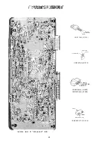
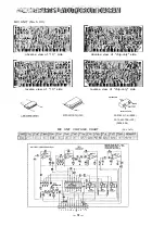
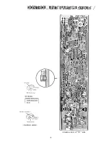
Page 15: ...20 32 HD404418A01F 02003 obverse view of 1C side 14...

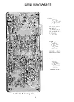
Page 16: ...S obverse view of 1C side 15 ANODE 1 CATHOOE 1...

Page 17: ......

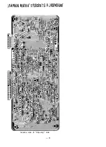
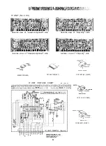
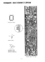
Page 18: ...PA UNIT No 7 XX obverse view of component side reverse view of component side 17...

Page 19: ...obverse view of chip only side reverse view of chip only side 18...

Page 20: ...19...

Page 21: ...MAIN UNIT 20...

Page 22: ...21 e s A...

Page 23: ...22...

Page 24: ...ts re placed and the need for realignment deter mined to be absolutely necessary The following test equipment and thorough familiarity with its correct use is necessary for complete realignment Correc...

Page 25: ...ne the transceiver to 430 MHz 432 MHz for Version D and while receiving adjust TC301 on the VCO Unit for at least 0 8V 1 0V for Version D c Retune the transceiver to the frequency indicated below and...

Page 26: ...he center of the band and set the LOW button to the high power position b Adjust L701 for maximum power output at least 36 watts 2 Power Output a With the transceiver tuned to the center of the band s...

Page 27: ...tch the coun ter indication with the transceiver frequency 4 Deviation a Set the AF generator for 25mV output at 1 kHz Adjust VR1003 for 4 5 kHz deviation on the Deviation Meter b Reduce the AF genera...

Page 28: ...01 and CVI 001 in that order for maximum S meter indication Reduce the injection level if necessary to keep the S meter near midrange 2 S Meter Calibration a At the center of the band set the signal g...

Page 29: ...49 R1050 R1051 R1052 R1053 R1054 R1055 R1056 R1057 R1064 R1065 PTH1001 VR1001 R1002 VR1003 VR1004 VR1005 VR1006 VR1007 C1003 C1004 C1005 C1006 C1007 C1008 C1009 C1010 C1011 C1012 C1013 C1014 C1015 C10...

Page 30: ...17 C418 L401 TP401 K Symbol No Q501 502 Q503 R501 R502 R503 R504 R505 R506 R507 R508 R509 R510 R511 R512 R513 R514 R515 R516 R517 R518 R519 R520 R521 R522 H7900180 J24205101 J24205101 J24205473 J24205...

Page 31: ...50V 220pF B 25V 0 022uF B 25V O luF B 25V 0 022uF B 25V 0 022uF B 25V 0 022uF B 50V O OOluF B 25V O luF B 25V 0 033uF B 25V O luF K Aai iS SNsse e Device FMS1 T98 2SC1623 T2B L6 2SB624 T2B BV4 2SB624...

Page 32: ...10W 8 2k ohm 1710W 56k ohm 1 10W 10k ohm 1710W 270k ohm 1 10W 1k ohm 1 10W 2 2k ohm 1 10W 22k ohm 1 10W 22k ohm 1 10W 39k ohm 1 10W 10k ohm 1 10W 10k ohm 1 10W 100k ohm 1 10W 100k ohm 1 10W 1k ohm 1...

Page 33: ...pF 16V lOuF CH 50V 4pF CH 50V 6pF B 50V 470pF B 50V 470pF CH 50V lOOpF CH 50V J pF CH 50V lOpF CH 50V 0 5pF CH 50V pF B 50V 470pF CH 50V 12pF CH 50V 12pF CH 50V 8pF B 50V 470pF B 50V 470pF CH 50V 6pF...

Reviews: