Alignment
ALIGNMENT-23
FT-99
1
Technical Supplement
Set the VFO-A frequency to 439.90 MHz in the
C4FM mode.
Press and hold the PTT button, then rotate the
[CLAR/VFO-B] knob for 4.5 kHz ±0.2 kHz on
the Deviation Meter.
Release the PTT button, then press and hold
in the [MENU(SETUP)] button for one second
to save the new setting and exit the alignment
mode.
IDD Meter Adjustment
Connect the 50-Ohm Dummy Load and Watt-
meter to the “HF/50 MHz” ANT jack.
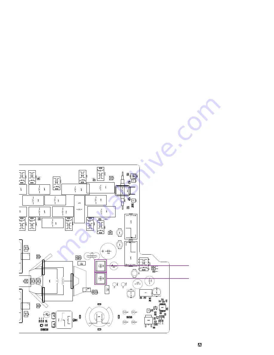
Remove the jumper that is connected between
J4006 and J4007 on the HF-PA-Unit, then con-
nect the DC ammeter (20-A range) between
J4006 and J4007.
Press and hold in the [A=B], [A/B], and [FAST]
keys, while turning the radio on, to enter the
alignment mode.
Rotate the [MULTI] Dial knob to select the
alignment menu item to “22-01 IDD MTR".
Set the VFO-A frequency to 14.200 MHz in the
CW mode.
Press and hold the PTT button, then rotate the
[CLAR/VFO-B] knob so the IDD meter reading
is the same as the DC ammeter.
Press the PTT button, then press the [F(M-LIST)]
key while pressing and holding in the PTT
button.
Release the PTT button, then press and hold
in the [MENU(SETUP)] button for one second
to save the new setting and exit the alignment
mode.
J4006
J4007
Summary of Contents for FT-991A
Page 10: ...BLOCK DIAGRAM 1 FT 991 Technical Supplement Block Diagram...
Page 11: ...CONNECTION DIAGRAM 1 FT 991 Technical Supplement Connection Diagram...
Page 36: ...FT 991 Technical Supplement MAIN 1 Circuit Diagram MAIN Unit...
Page 37: ...FT 991 Technical Supplement MAIN 2 Parts Layout side A MAIN Unit 1 2 3 4 5 A B C D E F G...
Page 38: ...FT 991 Technical Supplement MAIN 3 Parts Layout side B MAIN Unit 1 2 3 4 5 a b c d e f g...
Page 68: ...FT 991 Technical Supplement PLL 1 PLL Unit Circuit Diagram...
Page 69: ...FT 991 Technical Supplement PLL 2 PLL Unit Parts Layout side A side B 1 2 3 A B C...
Page 73: ...FT 991 Technical Supplement EDSP 1 Circuit Diagram EDSP Unit...
Page 79: ...FT 991 Technical Supplement CNTL 1 CNTL Unit Circuit Diagram...
Page 80: ...FT 991 Technical Supplement CNTL 2 CNTL Unit Parts Layout side A A B C D E F G 1 2 3 4...
Page 81: ...FT 991 Technical Supplement CNTL 3 CNTL Unit Parts Layout side B a b c d e f g 1 2 3 4...
Page 87: ...FT 991 Technical Supplement HF PA 1 HF PA Unit Circuit Diagram...
Page 88: ...FT 991 Technical Supplement HF PA 2 HF PA Unit Parts Layout side A 1 2 3 4 A B D F G E C 5...
Page 89: ...FT 991 Technical Supplement HF PA 3 HF PA Unit Parts Layout side B 1 2 3 4 a b d f g e c 5...
Page 96: ...FT 991 Technical Supplement V_U PA 1 Circuit Diagram V_U PA Unit...
Page 97: ...FT 991 Technical Supplement V_U PA 2 V_U PA Unit Parts Layout side A 1 2 3 A B C D E F G H...
Page 98: ...FT 991 Technical Supplement V_U PA 3 V_U PA Unit Parts Layout side B 1 2 3 a b c f h j d e g i...
Page 105: ...FT 991 Technical Supplement PANEL 1 Circuit Diagram PANEL Unit...
Page 113: ...FT 991 Technical Supplement TUNER 1 TUNER Unit Circuit Diagram...
Page 114: ...FT 991 Technical Supplement TUNER 2 TUNER Unit Parts Layout side A 1 2 3 4 A B C D E F G H...
Page 115: ...FT 991 Technical Supplement TUNER 3 TUNER Unit Parts Layout side B...
Page 119: ...JACK 1 JACK Unit Circuit Diagram FT 991 Technical Supplement...
Page 120: ...JACK 2 JACK Unit Parts Layout side A side B FT 991 Technical Supplement...
Page 122: ...FT 991 Technical Supplement SCP 1 Circuit Diagram SCP Unit...
Page 123: ...FT 991 Technical Supplement SCP 2 Parts Layout SCP Unit side A side B...
Page 127: ...FT 991 Technical Supplement DSP 1 DSP Unit Circuit Diagram...
Page 128: ...FT 991 Technical Supplement DSP 2 DSP Unit Parts Layout side A side B...


