(2) BNC
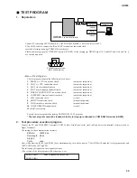
· Connect AD824 word clock out and DA824 word clock in.
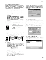
· Insert MY8-AE card into the slot and connect to DSA1 via the D-sub-cannon converter box.
· Set AD824 word clock settings to BNC.
· Set AD824 word clock settings to 44.1 kHz and 48 kHz.
2-6
Fs operating range
· Connect the oscillator to AD824 word clock in.
· Set AD824 word clock settings to BNC.
(1) Fs=50.88 kHz (48 kHz+6 %)
· Set the oscillator to 50.88 kHz.
· Conduct a listening test for one minute to check that there is no noise.
(2) Fs=39.69 kHz (44.1 kHz-10 %)
· Set the oscillator to 39.69 kHz.
· Make the same input as 2-6 (1) and confirm that the same output level is attained. Or, conduct a listening test for one minute
to check that there is no noise.
3.
Sound
Perform a listening test to confirm the following items.
· INPUT1 to 8
4.
Initialization
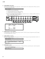
While pressing the [SEL4] key and [+48V] key, turn on the power switch. The system will start up and initialize.
Others, the SW that are not controlled by the CPU are as follows.
· +48V MASTER:
OFF
· WORD CLOCK IN 75 ohms:
ON
· PC RS422:
RS422
AD824
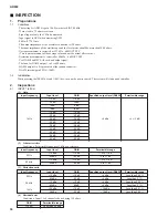
38
WORD CLOCK
Permissible range
44.1 kHz
48 kHz
Less than 5 nsec
Less than 5 nsec
Input frequency
Input level (AD824)
Output level
Permissible range
1 kHz
+10 dBu
+4 dBu
+4 +/-1 dBu
Summary of Contents for AD824
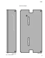
Page 22: ...MAIN Circuit Board B B 3NA V579130 AD824 22 ...
Page 23: ...E B B MAIN MYSL 3NA V579130 MYSL Circuit Board AD824 23 Pattern side Pattern side ...
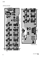
Page 24: ...3NA V579110 INPUT BAL 1 2 3 4 5 6 7 8 1 HA Circuit Board C C AD824 24 ...
Page 25: ...AD824 25 3NA V579110 to MAIN CN903 1 C C to JK CN202 to JK CN102 to DC CN007 Component side ...
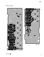
Page 26: ...HA Circuit Board 3NA V579110 1 D D AD824 26 ...
Page 27: ...3NA V579110 1 D D AD824 27 Pattern side ...
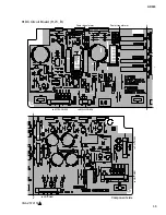
Page 30: ...AD824 30 AD Circuit Board 3NA V579120 F F ...
Page 31: ...AD824 31 JK Circuit Board F F AD JK 3NA V579120 Pattern side Pattern side ...
Page 33: ...PN Circuit Board 3NA V579100 1 H H H H AD824 33 Pattern side ...


