AD824
39
1.
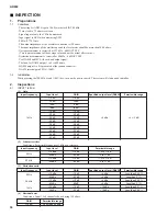
Reparations
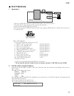
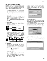
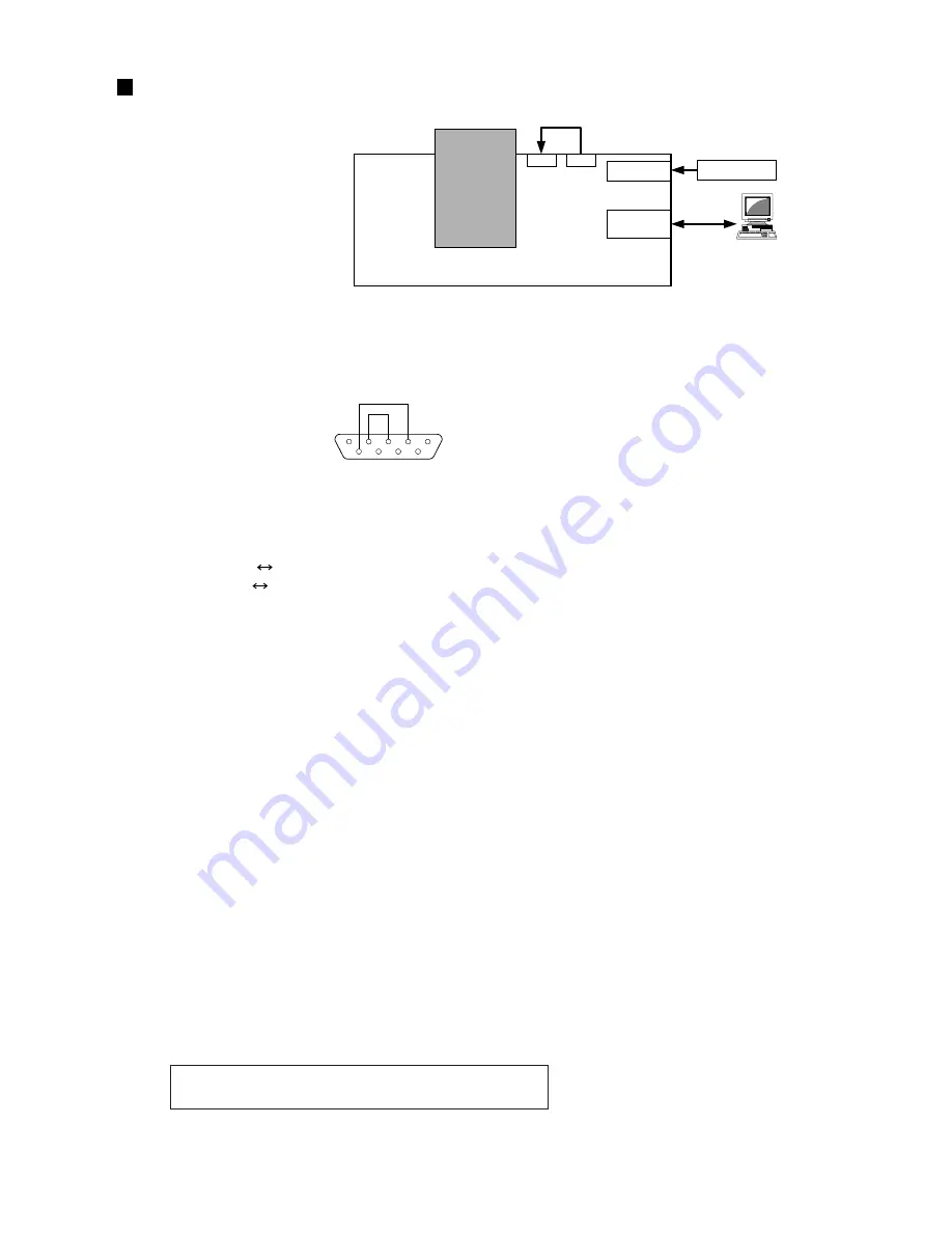
· Connect PC (operating MS Windows) to COM PC/RS422 terminal. The switch selects the PC.
· EUse a BNC cable to connect the IN and OUT terminals of the world clock.
· Insert the slot inspection jig (TX800810) into the slot.
· EInsert the turning jig into COM RS422 terminal (CN908). In the turning jig, DSUB 9 pins No. 2 and No3, and No.4 and No. 6
are shorted and used.
<Menu of Test Program>
The test program inspects the following eleven items.
1. SRAM
CPU connection check
(automatic inspection)
2. SLOT
CPU connection check
(automatic inspection)
3. SLOT clock relationship check
(automatic inspection)
4. SLOT power supply peripheral check
(automatic inspection)
5. WORD CLOCK IN/OUT connection check
(automatic inspection)
6. COM RS422 terminal connection check
(automatic inspection)
7. LED connection check
(visual)
8. SWITCH connection check
(manual inspection)
9. GAIN encoder connection check
(manual inspection)
10. COM PC/RS422 terminal check
(visual)
11. Initializes memory
Execute the test program after loading DA824DIAG/V1.00 program.
* The test program cannot be loaded while the turning jig is attached to COM RS422 terminal (CN908).
2.
Test procedure execution program
Connect the PC and COM RS422 terminals/ CN903 with a Dsub 9-pin serial cross cable and start the terminal software (such as
Hyper Terminal).
The setting for the communication format is
Bit Rate:
38400 bps
Data length: 8 bits
Stop bit:
1
Parity:
none
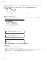
Next, while pressing [SEL3] and [SEL8] keys simultaneously, turn on the power. The AD824 will enter the test program mode and
“d00” will flash on the 7segLED.
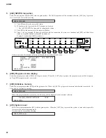
The following will appear on the terminal software.
( The version of the test program will be shown as x.xx.)
TEST PROGRAM
WORD CLOCK
PC
COM
PC/RC422
AD824
SLOT INSPECTION JIG
IN
COM RS422
(CN908)
(CN907)
TURNING JIG
OUT
1
2
3
4
6
7
8
9
5
DSUB9P Female Connecter
(DELC-J9SAF10L9 etc.)
AD824_DIAG>
AD824 Diagnosis version Vx.xx
AD824_DIAG>
Summary of Contents for AD824
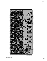
Page 22: ...MAIN Circuit Board B B 3NA V579130 AD824 22 ...
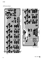
Page 23: ...E B B MAIN MYSL 3NA V579130 MYSL Circuit Board AD824 23 Pattern side Pattern side ...
Page 24: ...3NA V579110 INPUT BAL 1 2 3 4 5 6 7 8 1 HA Circuit Board C C AD824 24 ...
Page 25: ...AD824 25 3NA V579110 to MAIN CN903 1 C C to JK CN202 to JK CN102 to DC CN007 Component side ...
Page 26: ...HA Circuit Board 3NA V579110 1 D D AD824 26 ...
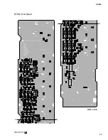
Page 27: ...3NA V579110 1 D D AD824 27 Pattern side ...
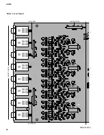
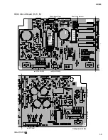
Page 30: ...AD824 30 AD Circuit Board 3NA V579120 F F ...
Page 31: ...AD824 31 JK Circuit Board F F AD JK 3NA V579120 Pattern side Pattern side ...
Page 33: ...PN Circuit Board 3NA V579100 1 H H H H AD824 33 Pattern side ...

