AD824
4
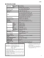
*1. 24-bit linear, 128-times oversampling A/D converters.
*2. XLR-type connectors are electronically balanced (pin 1 = ground, pin 2 = hot, pin 3 = cold).
*3. TRS phone jacks are electronically balanced (tip = hot, ring = cold, sleeve = ground).
*
Where dB represents a specific voltage, 0 dB is referenced to 0.775 V rms.
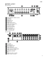
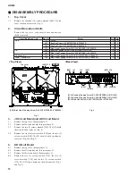
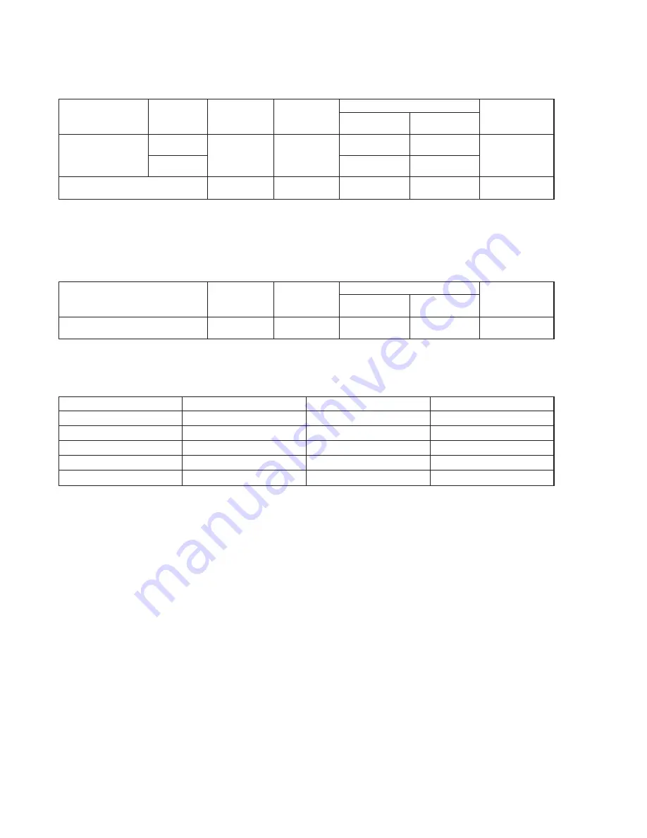
Analog Input
Connection
GAIN
Actual Load
Impedance
For Use
with
Nominal
Connector
Input Level
Nominal
Max.
before clip
INPUT 1–8 *
1
INSERT IN 1–8
3k
Ω
lines
10k W
50–600
Ω
mics &
600
Ω
lines
600
Ω
lines
-62 dB
+10 dB
-62 dB
(615
µ
V)
+10 dB
(2.45 V)
+10 dB
(2.45 V)
-48 dB
(3.08 mV)
+24 dB
(12.28 V)
+24 dB
(12.28 V)
XLR-3-31 type
(balanced)*
2
TRS phone jack
(balanced)*
3
*1. TRS phone jacks are electronically balanced (tip = hot, ring = cold, sleeve = ground).
*
Where dB represents a specific voltage, 0 dB is referenced to 0.775 V rms.
Analog Output
Connection
Actual Source
Impedance
For Use
with
Nominal
Connector
Output Level
Nominal
Max.
before clip
INSERT OUT 1–8
150
Ω
10k
Ω
lines
+10 dB
(2.45 V)
+24 dB
(12.28 V)
TRS phone jack
(balanced)*
1
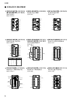
Digital I/O
Connection
COM PC/RS422
COM RS422
WORD CLOCK IN
WORD CLOCK OUT
SLOT
Format
—
—
—
—
mini YGDAI
Level/Impedance
RS232C/RS422
RS422
TTL, 75
Ω
(ON/OFF)
TTL, 75
Ω
—
Connector
9-pin D-sub (male)
9-pin D-sub
BNC
BNC
—
Summary of Contents for AD824
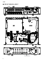
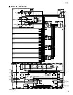
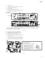
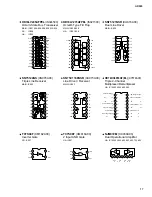
Page 22: ...MAIN Circuit Board B B 3NA V579130 AD824 22 ...
Page 23: ...E B B MAIN MYSL 3NA V579130 MYSL Circuit Board AD824 23 Pattern side Pattern side ...
Page 24: ...3NA V579110 INPUT BAL 1 2 3 4 5 6 7 8 1 HA Circuit Board C C AD824 24 ...
Page 25: ...AD824 25 3NA V579110 to MAIN CN903 1 C C to JK CN202 to JK CN102 to DC CN007 Component side ...
Page 26: ...HA Circuit Board 3NA V579110 1 D D AD824 26 ...
Page 27: ...3NA V579110 1 D D AD824 27 Pattern side ...
Page 30: ...AD824 30 AD Circuit Board 3NA V579120 F F ...
Page 31: ...AD824 31 JK Circuit Board F F AD JK 3NA V579120 Pattern side Pattern side ...
Page 33: ...PN Circuit Board 3NA V579100 1 H H H H AD824 33 Pattern side ...


