A
1
2
3
4
5
6
7
8
9
B
C
D
E
F
G
H
I
J
K
L
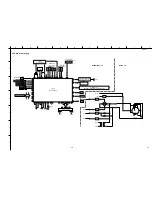
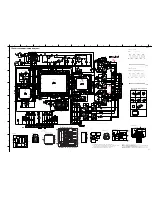
AV-S77C SCHEMATIC DIAGRAM (OPERATION)
43
AV-S77
★
All voltage are measured with a 10MΩ /V DC electric volt meter.
★
Components having special characteristics are marked
s
and must be replaced
with parts having specifications equal to those originally installed.
★
Schematic diagram is subject to change without notice.
Page 42
FROM MAIN
B7
Page 44
FROM DSP
C7
Page 42
FR
OM MAIN
A6
IC201 : S-29390AFJA
CMOS 4kbit Serial EEPROM
5
2
7
6
8
1
3
4
DI
Vcc
GND
DO
TEST
NC
CS
SK
Memory array
Address decoder
Data register
Output buffer
Mode decode logic
Clock generator
2SA1037K
DTA144EK
DTC144EK
ISS355
UDZ5.1B
MTZ6.2B
PIN CONNECTION DIAGRAM OF TRANSISTORS, DIODES AND ICS.
B
E
C
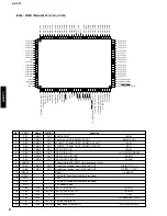
M30218FCFP
S-29390AFJA
1
4
8
1
30
31
50
51
80
81
100
Anode
Cathode
Point
3
Pin 13 of IC200
Point
4
emitter of Q209
and collector of Q208
POWER ON
(Connect the power cord)
POWER OFF
(Disconnect the power cord)
Q209 E
Q208 C
C
Ch 1
Ch 2
5.1
5.1
0.2
5.1
0
Point
C
VCC of IC4
and OUT of IC4
Point
B
Pin 129 of IC3
POWER ON
(Connect the power cord)
POWER OFF
(Disconnect the power cord)
IC4 VCC
IC4 OUT
4.7
4.7
-11.4
4.7
4.7
-11.4
4.7
4.7
-0.4
~
-25.1
~
~
~
~
~
~
-25.3
4.5
5.0
1.7
4.7
4.7
0.8
4.7
0
4.7
4.7
4.7
~
-25.1
-20.4
-20.4
~
~
~
~
~
~
-25.1
~
-25.1
~
~
~
~
~
~
~
~
~
~
~
~
~
~
~
~
~
~
~
~
~
~
~
~
~
~
~
~
~
~
~
~
~
~
~
-20.4
-20.4
~
~
~
~
~
~
~
~
~
~
~
~
~
~
~
~
~
0
~
4.7
~
~
~
~
~
~
~
~
~
~
~
~
~
~
~
~
~
~
~
~
~
~
~
~
0
4.7
4.7
0
0
0
0
4.7
4.7
4.7
0
0
0
0
6.2
6.2
0
11.5
11.4
10.8
6.8
0
0
4.7
0.4
0
0
0
0
4.7
0
0
4.7
0
0
0
0
4.8
4.7
0.6
4.7
4.7
4.6
4.7
0
4.8
0
1.6
4.7
2.0
0
2.3
4.7
4.7
4.7
0
4.8
4.8
4.8
0
0
0
4.7
4.7
3
2
B
A
5
6
SYSTEM CONRTOL
EEP ROM
RESET

