background image

CDX-497/CDX-397

3

CDX-497/CDX-397

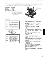
WARNING

Laser Diode Properties

Material:

GaAlAs

Wavelength:

780 nm

Emission duration:

continuous

Laser output:

max. 44.6 

µ

W *

* This output is the value measured

at a distance of about 200 mm from
the objective lens surface on the
Optical Pick-up Block.

Optical Pick-up

2) The laser power level can be adjusted with the VR on the pick-up PWB. However, this level has been set by the factory

prior to shipping from the factory. Do not adjust this laser level control unless instruction is provided elsewhere in this
manual. Adjustment of this control can increase the laser emission level from the device.

Summary of Contents for CDX-497

Page 1: ...gineering and service departments of YAMAHA are continually striving to improve YAMAHA products Modifications are therefore inevitable and specifications are subject to change without notice or obligation to retrofit Should any discrepancy appear to exist please contact the distributor s Service Division WARNING Static discharges can destroy expensive components Discharge any static electricity yo...

Page 2: ...ンダにはいくつかの種類がありますが 修理時には下記の ような無鉛ハンダの使用を推奨します Sn Ag Cu 錫 銀 銅 Sn Cu 錫 銅 Sn Zn Bi 錫 亜鉛 ビスマス 注意 無鉛ハンダの融点温度は通常の鉛入りハンダに比べ30 40 程度高くなっていますので それぞれのハンダに合ったハン ダごてをご使用ください All of the P C B s installed in this unit are soldered using the lead free solder Among some types of lead free solder currently available it is recommended to use one of the following types for the repair work Sn Ag Cu tin silver copper S...

Page 3: ...200 mm from the objective lens surface on the Optical Pick up Block Optical Pick up 2 The laser power level can be adjusted with the VR on the pick up PWB However this level has been set by the factory prior to shipping from the factory Do not adjust this laser level control unless instruction is provided elsewhere in this manual Adjustment of this control can increase the laser emission level fro...

Page 4: ...CDX 497 CDX 397 4 CDX 497 CDX 397 ...

Page 5: ... 5 Do not use freon propelled chemicals These can generate electrical charges sufficient to damage ES devices 6 Do not remove a replacement ES device from its protective package until immediately before you are ready to install it Most replacement ES devices are packaged with leads electrically shorted together by conductive foam aluminum foil or compa rable conductive material 7 Immediately befor...

Page 6: ...CDX 497 CDX 397 6 CDX 497 CDX 397 FRONT PANELS REAR PANELS CDX 497 R model CDX 497 R T K A B G J models CDX 397 R T A B G models CDX 497 T model CDX 497 K model ...

Page 7: ...CDX 497 CDX 397 7 CDX 497 CDX 397 CDX 497 A model CDX 497 B G models CDX 497 J model CDX 397 R model CDX 397 T model ...

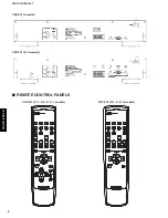
Page 8: ...CDX 497 CDX 397 8 CDX 497 CDX 397 REMOTE CONTROL PANELS CDX 397 A model CDX 397 B G models CDX 497 R T K A B G J models CDX 397 R T A B G models ...

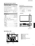
Page 9: ...消費電力 13 W Dimensions W x H x D 寸法 幅 高さ 奥行き 435 x 87 x 287 mm 17 1 8 x 3 7 16 x 11 5 16 Weight 質量 3 5 kg 7 lbs 11 oz Finish 仕上げ CDX 497 Gold color T K J models Black color R A G models Titanium color R B G models CDX 397 Gold color T model Black color R T A G models Titanium color R B G models DIMENSIONS 435 17 1 8 276 10 7 8 17 11 16 4 3 16 70 2 3 4 87 3 7 16 287 11 5 16 7 1 4 1 5 3 2 4 6 7 8 FRON...

Page 10: ...故障の場合は 各ユニットを交換してください CDメカニズム MAIN P C B FRONT P C B REPAIR NOTES 修理上の留意点 HOW TO MANUALLY EJECT THE TRAY 手動でトレーを開く方法 a Turn the unit bottom up b Using a flatblade screwdriver turn the loading cam 90 degrees in the direction indicated by an arrow in the figure c Gently pull the tray out a 本機を上下反転します b マイナスドライバーでローディングカムを図に示す矢 印の方向に90度回転します c トレーをそっと引き出します Tray トレー Loading cam ローディングカム Tray トレー Flat...

Page 11: ...onnectors MAIN 2 P C B 35 2 Remove CN43 Remove 2 screws 53 P C B to rear panel Remove FRONT 5 P C B FRONT 5 P C B 31 5 R model Remove CN41 FRONT 2 P C B CN41 MAIN P C B and CN44 Remove CN43 R model P C B to rear panel Remove 1 screws 56 P C B to bottom frame Remove 3 screws 55 P C B to bottom frame FRONT 2 P C B 31 2 Remove 2 screws 53 P C B to front panel ass y Remove FRONT 4 P C B FRONT 4 P C B ...

Page 12: ...AIN 1 P C B を取り外し ます MAIN 1 P C B 35 1 FRONT 4 P C B 31 4 ネジ 53 1本を外します FRONT 1 P C B を取り 外します FRONT 1 P C B 31 1 ネジ 53 1本を外します FRONT 4 P C B を取り 外します FRONT 3 P C B を取り外 します ネジ 54 1本を外します FRONT 3 P C B 31 3 CN21 23を外します 底面のネジ 57 4本を外します CDメカニズムを取り外します CDメカニズム 38 フロントパネルASS Y CN41 FRONT 2 P C B CN41 MAIN P C B CN44を外します 底面のネジ 55 3本を外します 底面のネジ 56 1本を外します FRONT 2 P C B を取り外します FRONT 2 P C B 31 2 Moun...

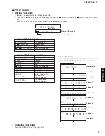
Page 13: ...traverse reverse Move traverse forward 1 Function list of panel keys F F F F F OPEN CLOSE W W W W W PLAY D D D D D PAUSE A A A A A STOP T T T T T SKIP Y Y Y Y Y SKIP TIME INFO SPACE RANDOM OUTPUT LEVEL OUTPUT LEVEL Tray open close Playback Pause Stop Move traverse reverse Move traverse forward Check FL display 1 EEPROM write read test Spindle servo on off Output level up CDX 497 model Output level...

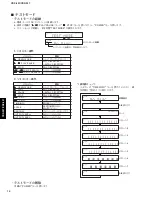
Page 14: ...KIP SEARCH トレイ オープン クローズ 再生 DISC挿入時 一時停止 DISC再生時 停止 DISC再生時 トラバース内周移動 トラバース外周移動 パネルキー 機能 1 パネルキー操作 F F F F F OPEN CLOSE W W W W W PLAY D D D D D PAUSE A A A A A STOP T T T T T SKIP Y Y Y Y Y SKIP TIME INFO SPACE RANDOM OUTPUT LEVEL OUTPUT LEVEL トレイ オープン クローズ 再生 DISC挿入時 一時停止 DISC再生時 停止 DISC再生時 トラバース内周移動 トラバース外周移動 表示器チェック 1 EEPROM書き込み 読み取りテスト スピンドルサーボオン オフ 出力レベルを上げる 出力レベルを下げる パネルキー 機能 1 表示器チェック リモコン...

Page 15: ...ion flag output pin H if the AOUT pin outputs an uncorrectable symbol in C2 correction CD Processor Status signal output Pin for outputting the playback frame sync signal Emphasis fiag output pin ENPH on H EMPH off L The output polarity can be switched using a command LOCk signal Pin for monitoring signals in the DSP Output pin for zero detection flag for the 1 bit DAC Pin for outputting subcode P...

Page 16: ...5AI F I 3I F I O 3I F I O 3I F I O 3I F I O 3I F O 3I F O 3I F O 3I F O 3I F I 3I F I 3I F I 3I F O 3AI F O 3AI F O 3AI F Remark IC21 TC94A54 MAIN P C B DSP Pin No Pin name Function Pin name 70 71 72 73 74 75 76 77 78 79 80 81 82 83 84 85 86 87 88 89 90 91 92 93 94 95 96 97 98 99 100 LPFN LPFO PVREF VCOF VCOREF PVSS3 SLCO RFI RFRPI RFEQO RESIN VRO VMDIR TESTR INVSEL AGCI AGCI RFO PNSEL EQSET RVDD3...

Page 17: ...0 27 28 29 are connected to PW GND FIN 8 9 10 27 28 29 are connected to PW GND FIN 8 9 10 27 28 29 are connected to PW GND FIN Input for ch2 Open Open Supply voltage terminal for ch 1 ch2 Inverted output for ch2 Non inverted output for ch2 Inverted output for ch1 Non inverted output for ch1 Non inverted output for ch3 Inverted output for ch3 Non inverted output for ch4 Inverted output for ch4 Supp...

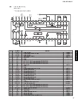
Page 18: ...VOLUME CONTROL VOLUME CONTROL INTERPOLATION FILTER INTERPOLATION FILTER DAC DAC ANALOG FILTER ANALOG FILTER MIXER FILT AOUTA AOUTA AOUTB AOUTB LRCK SCLK SDATA CMOUT BMUTEC AMUTEC M3 M1 SDA CDIN M2 CL CCLK M0 AD0 CS RST RST AOUTA VL AOUTA SDATA VA SCLK AGND LRCK AOUTB MCLK AOUTB M3 BMUTEC SCL CCLK M2 CMOUT SDA CDIN M1 FILT AD0 CS M0 2 19 3 18 4 17 5 16 6 15 7 14 8 13 9 12 10 11 ...

Page 19: ... Mute Control output The Mute Confrol pin goes high during power up initialization reset muting power down or if the master clock to left right clock frequency ratio is incorrect Differential Analog Output Outputs The full scale differential analog output level is specified in the Analog Characteristics specification table Ground Input Analog Power Input Positive power for the analog section 7 8 9...

Page 20: ... IN CDX 497 model CD Mechanism MAIN See page 25 SCHEMATIC DIAGRAM FRONT See page 26 SCHEMATIC DIAGRAM DIGITAL OUT COAXIAL OPTICAL JK75 JK52 IC75 IC73 IC74 IC72 IC71 JK73 LINE OUT L R IC22 IC21 X201 IC51 X501 RS51 SW41 Q401 IC45 IC43 IC44 IC42 IC41 D401 403 D402 404 D405 406 T401 FL51 ...

Page 21: ...VP_ON 13 1 9V AGND 9V P_MUTE PWR_ON 8V MGND VDD ST 5V FL FL VP FLT_ON 13 1 6 1 NC KEY2 KEY1 GND GND ST 5V VFD DI VFD CLK VFD CE VFD RST REMO FL VP FL NC STBY LED KEY2 KEY1 DGND DGND ST 5V VFD DI VFD CLK VFD CE VFD RST REMO FL VP FL VDD 1 14 15 2 1 15 1 5 1 7 1 6 1 7 16 2 1 14 15 2 9V 9V 9V AGND 9V PWR_ON FCS TRK TRK FCS LD PD LD VR LD LD PDIC GND PDIC F PDIC C PDIC B PDIC A PDIC D PDIC E PDIC VCC ...

Page 22: ...IT BOARDS FOR INFORMATION ONLY NO SERVICE PARTS WILL BE AVAILABLE MAIN 1 P C B Top view MAIN 2 CN43 FRONT 2 CN41 FRONT 3 BN71 FRONT 1 BN52 CD Mechanism CDX 497 model CDX 497 model CDX 497 model DIGITAL OUT OPTICAL LINE OUT L R COAXIAL MAIN 2 P C B Top view MAIN 1 CN42 ...

Page 23: ...A B C D E F G H I J 1 2 3 4 5 6 CDX 497 CDX 397 23 7 CDX 497 model MAIN 1 P C B Bottom view MAIN 2 P C B Bottom view ...

Page 24: ...ONT 2 P C B Top view FRONT 4 BN42 FRONT 5 BN43 R model MAIN 1 CN41 T K A B G J models R model FRONT 3 P C B Top view MAIN 1 CN71 CDX 497 model PHONES L R FRONT 4 P C B Top view FRONT 2 CN42 POWER ON OFF FRONT 5 P C B Top view FRONT 2 CN43 VOLTAGE SELECTOR R model 220 240 VOLTS 110 120 VOLTS ...

Page 25: ...OR INFORMATION ONLY NO SERVICE PARTS WILL BE AVAILABLE MAIN to FRONT 1 _CN52 Page 26 D2 to FRONT 2 _CN41 Page 26 B4 to FRONT 3 _BN71 To CD Machanism To CD Machanism AUDIO OUT DIGITAL OUT Page 26 H2 L COAXIAL OPTICAL R To CD Machanism MAIN 2 MAIN 1 CDX 497 model CDX 497 model ...

Page 26: ... 26 FRONT FRONT 1 FRONT 4 FRONT 2 FRONT 5 FRONT 3 to MAIN 1 _CN52 Page 25 B7 to MAIN 1 _CN71 Page 25 H6 to MAIN 1 _CB41 Page 25 C7 R model R model CDX 497 model POWER ON OFF PHONES VOLTAGE SELECTOR 220 240 VOLTS 110 120 VOLTS T K A B G J models AC IN ...

Page 27: ...CDX 497 CDX 397 27 MEMO MEMO MEMO MEMO ...

Page 28: ...7 model CDX 497 model CDX 497 model R model R model 1 2 3 4 5 6 7 6 7 9 21 24 25 31 1 31 3 31 4 31 2 31 5 35 1 35 2 38 38 1 39 200 201 202 51 51 52 52 53 53 54 61 61 60 55 55 56 57 57 56 58 58 59 53 Note The replacement battery cover is not available CDX 497 model CDX 397 model 72 71 ...

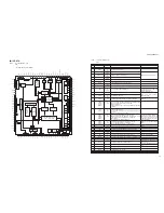
Page 29: ...IN COP11855C PCB メイン 38 AAX78140 CD MECHANISM CJDKSL2130CCMZ CDメカニズム 38 1 AAX78500 BELT 9A07980900 ベルト s 39 AAX74330 POWER CABLE 2m CJA2J049ZA J 電源コード 04 s 39 AAX74340 POWER CABLE 2m CJA2L072ZA R 電源コード s 39 AAX74350 POWER CABLE 2m CJA2N047ZA T 電源コード s 39 AAX78680 POWER CABLE 2m CJA2D073Y K 電源コード s 39 AAX74360 POWER CABLE 2m CJA2S048ZA A 電源コード s 39 AAX78690 POWER CABLE 2m CJA2E086ZA B 電源コード s 39 AA...

Page 30: ...R OUTPUT LEVEL Q Q Q Q Q FILE ENTER W W W W W FILE G G G G G FOLDER OUTPUT LEVEL 79 01 79 11 79 12 79 13 79 14 79 15 79 16 79 17 79 18 79 19 79 10 79 0B 79 1E 79 1B 79 08 79 09 79 0C 79 0D 79 58 79 57 79 5D 79 0F 79 05 79 06 79 02 79 04 79 07 79 56 79 0A 79 55 79 69 79 1D 79 6C 79 3F 79 6B 79 6A 79 1C REMOTE CONTROL PANELS KEY CODE Key label Code CDX 497 R T K A B G J models CDX 397 R T A B G mode...

Reviews: