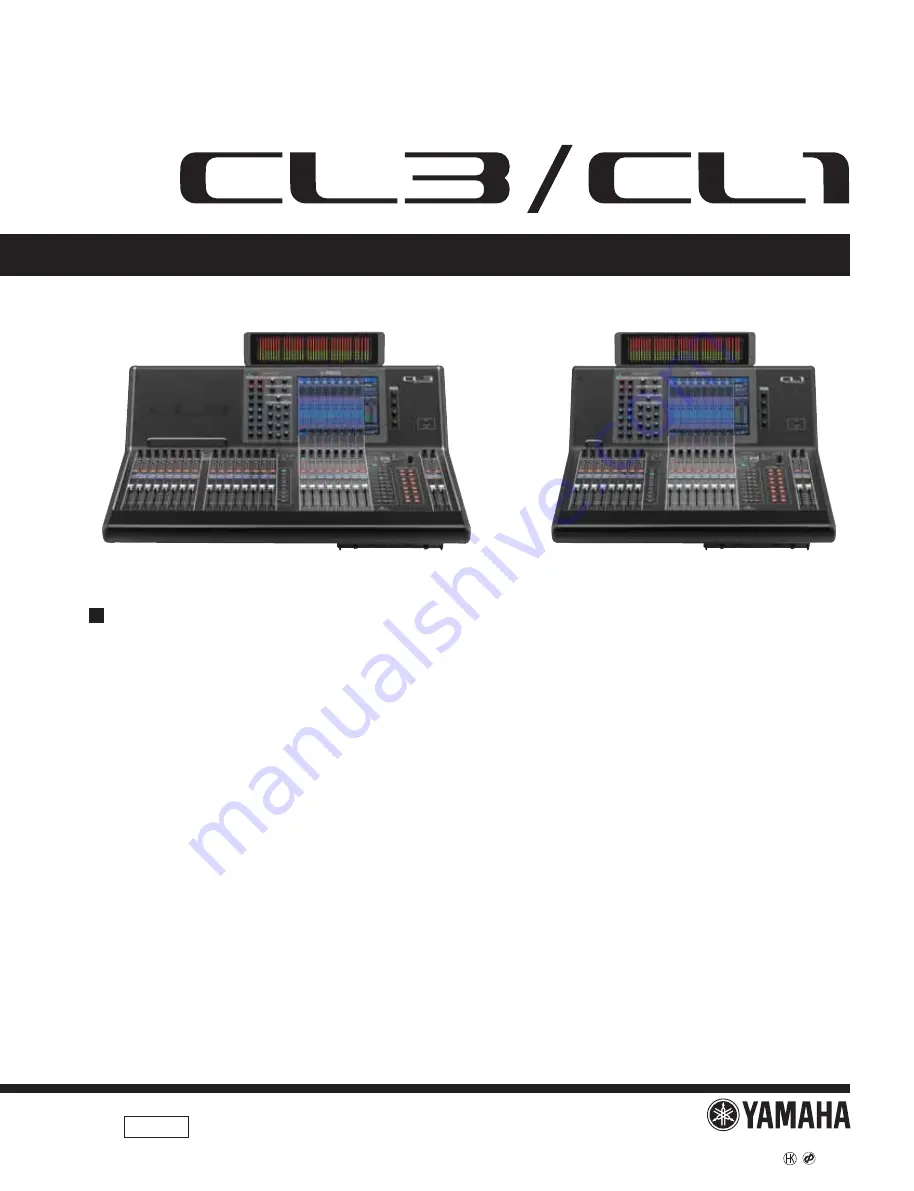
background image

SERVICE MANUAL

HAMAMATSU, JAPAN

PA

012056

Copyright (c) Yamaha Corporation. All rights reserved.  PDF  


  ’12.09

SPECIFICATIONS

(総合仕様)

  ................................. 4

PIN ASSIGNMENTS

(ピンアサイン表)

  ................... 6

DIMENSIONS

(寸法図)

  ............................................ 7

PANEL LAYOUT

(パネルレイアウト)

  ...................... 8

CL3 CIRCUIT BOARD LAYOUT

(ユニットレイアウト)

  ............................................. 14

CL1 CIRCUIT BOARD LAYOUT

(ユニットレイアウト)

  ............................................. 17

CL3 DISASSEMBLY PROCEDURE

(分解手順)

  .... 20

CL1 DISASSEMBLY PROCEDURE

(分解手順)

  .... 45

LSI PIN DESCRIPTION

(LSI 端子機能表)

  ............. 70

CIRCUIT BOARDS

(シート基板図)

  ....................... 93

INSPECTIONS

(検査)

  ................................... 122/127

SETTINGS FOR SHIPMENT

(出荷設定)

  ...... 126/131

SERVICE CHECK PROGRAM

(サービス検査プログラム)

  ............................ 132/148

UPDATING FIRMWARE

(FIRMWARE のアップデート) ....................... 164/165

INITIALIZATION

(イニシャライズ) ................ 166/167

TOUCH SCREEN CALIBRATION

(タッチスクリーンのキャリブレーション) .... 168/169

FADER CALIBRATION

(フェーダーキャリブレーション) ................... 170/171

 CONTENTS

(目次)

COLOR BAR AND CH NAME LCD CALIBRATION

(カラーバーと CH NAME LCD のキャリブレーション) ... 172/173

SCREEN SHOT

(スクリーンショット) ................ 174

UPDATING DANTE MODULE (Brooklyn2)

(DANTE モジュール (Brooklyn2) のアップデート) ... 175/177

DANTE SOUND OUTPUT CHECK

(DANTE 音出し検査) ...................................... 179/180

STARTING SEQUENCE

(起動シーケンス) ... 181/184

MEMORY INITIALIZATION(メモリ初期化) ......... 187

LIST OF FUNCTIONS OF DSP ICS OF DSP/FX CIRCUIT 
BOARD AND CORRESPONDING SDRAMS

(DSP/FX シートの各 DSP IC の機能と対応 SDRAM の一覧) .. 189

REQUIRED ITEMS FOR REPLACEMENT OF CPU 
CIRCUIT BOARD AND REPLACEMENT PROCEDURE

(CPU シート交換後に必要な項目と手順) ...... 192/193

PARTS LIST
BLOCK DIAGRAM

(ブロックダイアグラム)

OVERALL CONNECTOR CIRCUIT DIAGRAM

(総コネクタ接続回路図)

CIRCUIT DIAGRAM

(回路図)

MBCL SERVICE MANUAL

DIGITAL MIXING CONSOLE

 CL3 with MBCL

 CL1 with MBCL

OPTION

(オプション)  METER BRIDGE


MBCL

20120401-

オープンプライス

Summary of Contents for CL3

Page 1: ...TOUCH SCREEN CALIBRATION 168 169 FADER CALIBRATION 170 171 CONTENTS COLOR BAR AND CH NAME LCD CALIBRATION CH NAME LCD 172 173 SCREEN SHOT 174 UPDATING DANTE MODULE Brooklyn2 DANTE Brooklyn2 175 177 D...

Page 2: ...without notice or obligation to retrofit Should any discrepancy appear to exist please contact the distributor s Service Division WARNING Static discharges can destroy expensive components Discharge a...

Page 3: ...wires in the mains lead of this apparatus may not correspond with the coloured markings identifying the terminals in your plug proceed as follows The wire which is coloured GREEN and YELLOW must be c...

Page 4: ...Bu into 600 OMNI IN to OMNI OUT Input Gain Min Hum Noise 5 128dBu typ Equivalent Input Noise Input Gain Max 88dBu Residual output noise ST master off Dynamic Range 112dB typ DA Converter 108dB typ OMN...

Page 5: ...rating 5W Voltage control by software Input Terminals GAIN Actual Load Impedance For Use With Nominal Input Level Connector Sensitivity 1 Nominal Max before clip OMNI IN 1 8 66dB 10k 50 600 Mics 600...

Page 6: ...CT A 10 GND 22 DETECT B 11 GND 23 DETECT GND 12 GND Frame GND 1 2 3 4 5 6 7 8 9 3 1 2 1 1 1 0 1 14 15 16 1 7 1 8 0 2 9 1 21 22 23 Pin Signal Name Pin Signal Name 1 GPO1 9 G PO2 2 GPO3 10 GPO4 3 GPO5 1...

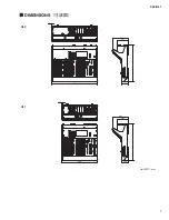
Page 7: ...7 CL3 CL1 DIMENSIONS CL3 CL1 648 15 201 130 299 667 839 15 201 130 299 667 Unit mm...

Page 8: ...logic section t SCENE MEMORY MONITOR section y USER DEFINED KNOBS section u USER DEFINED KEYS section i Master section o USB connector 1 Top Panel q w SELECTED CHANNEL e r Centralogic t SCENE MEMORY M...

Page 9: ...6 knobs e GAIN knob r PAN knob t DYNAMICS 1 knob y DYNAMICS 2 knob u HPF knob i EQ Q EQ FREQUENCY EQ GAIN knobs 2 Top Panel Details 2 1 Channel Strip section 2 2 SELECTED CHANNEL section SELECTED CHAN...

Page 10: ...s w Multifunction knob e SEL key r CUE key t Meter LEDs y ON key u Channel name display i Channel color indicator o Fader 2 3 Display section 2 4 Centralogic section Centralogic q w e r t y u i o q w...

Page 11: ...DEFINED knobs A D USER DEFINED keys 1 16 2 5 SCENE MEMORY MONITOR section SCENE MEMORY MONITOR 2 6 USER DEFINED KNOBS section USER DEFINED KNOBS 2 7 USER DEFINED KEYS section USER DEFINED KEYS q w y...

Page 12: ...12 q GAIN PAN ASSIGN knob w SEL key e CUE key r ON key t Channel name display y Channel color indicator u Fader 2 8 Master section 2 9 USB connector USB q w e r t y u q GAIN PAN ASSIGN w SEL e CUE r O...

Page 13: ...or y OMNI IN jacks u OMNI OUT jacks i Dante connectors o NETWORK connector 0 SLOT 1 3 1 DC POWER INPUT connector 2 AC IN connector 3 Power Switch 4 Grounding screw 3 Front Panel 4 Rear Panel q w r e q...

Page 14: ...5 ASSEMBLY U5 Ass y CONTROL PANEL U5 ASSEMBLY U5 Ass y REAR UPPER U5 SUB ASSEMBLY U5 Ass y CONTROL PANEL U5 ASSEMBLY U5 Ass y LCD U ASSEMBLY LCD U Ass y USB PNENR PNENL LCDC Some circuit boards may be...

Page 15: ...s y Bottom U5 Assembly U5 Ass y FRONT PAD ASSEMBLY U5 F Ass y U5 PN8 PN8 PN8 PN2 FD2 FD8CN FD8 FD8 PNM PNI SIDE PAD ASSEMBLY R Ass y R POWER SUPPLY ASSEMBLY Ass y AC ASSEMBLY AC SIDE PAD ASSEMBLY L As...

Page 16: ...RY JK CPU DSP DA FX DNTU TBPHN HAAD PS FAN ASSEMBLY PS Ass y LAMP CONNECTOR ASSEMBLY LAMP Ass y DANTE MODULE 64CH 64CH DNTU The ferrite cores which FFC cable passes through have been disused midway th...

Page 17: ...cuit boards may be different in color from those in the photo BOTTOM U7 ASSEMBLY U7 Ass y CONTROL PANEL U7 ASSEMBLY U7 Ass y REAR UPPER U7 SUB ASSEMBLY U7 Ass y CONTROL PANEL U7 ASSEMBLY U7 Ass y LCD...

Page 18: ...7 Ass y Bottom U7 Assembly U7 Ass y FRONT PAD ASSEMBLY U7 F Ass y U7 PN8 PN8 PN2 FD2 FD8CN FD8 PNM PNI SIDE PAD ASSEMBLY R Ass y R POWER SUPPLY ASSEMBLY Ass y AC ASSEMBLY AC SIDE PAD ASSEMBLY L Ass y...

Page 19: ...19 CL3 CL1 LITHIUM BATTERY JK CPU DSP DA FX DNTU TBPHN HAAD PS FAN ASSEMBLY PS Ass y LAMP CONNECTOR ASSEMBLY LAMP Ass y DANTE MODULE 64CH 64CH DNTU...

Page 20: ...CH MAME LCD or LCD assembly be sure to execute calibration of the replacement part When replacing the CPU circuit board execute updating and each calibration of the firmware For the details refer to...

Page 21: ...y 34 A 16 DC Circuit Board DC 34 A 17 OPT Circuit Board OPT 35 A 18 LAMP Connector Assembly LAMP Ass y 35 A 19 TBPHN Sheet Assembly TBPHN Ass y 35 A 20 Side Pad Assembly Ass y 36 B Disassembly Procedu...

Page 22: ...screws marked 150A on the rear panel first and then remove the twenty one 21 screws marked 150B and the ten 10 screws marked 160 Fig 2 1 U5 Ass y 6 1 1 150A 2 150B 21 160 10 2 Fig 2 2 150B 150B 150B 1...

Page 23: ...U5 Ass y L R 2 3 90 100 4 1 3 U5 Ass y 13 5 1 2 Lift the control panel U5 assembly from the rear side and fixit with the service stays L and R Photo 2 Photo 3 Don t open the control panel by more tha...

Page 24: ...th side pads outward in the arrow A direction so as not to cause damage to its top on both sides Photo 6 b Tighten the screw 1 in photo 6 while pushing both side pads in the arrow B direction c Tighte...

Page 25: ...m battery be sure to save all the internal setting data in on a USB memory After removing or replacing the lithium battery be sure to reset the time and date of the clock built in this unit Owner s Ma...

Page 26: ...ice stays See procedure 1 A 1 2 Remove the seven 7 screws marked 1110 the four 4 screws marked 1120 and the two 2 screws marked 150A The rear upper U5 sub assembly can then be removed Photo 9 A U5 Ass...

Page 27: ...service stays See procedure 1 A 2 2 Remove the two 2 hexagonal nuts marked N1 and the two 2 screws marked 1100c The PNMB circuit board can then be removed Photo 9 A 3 DCMS Circuit Board Time required...

Page 28: ...PU circuit board MRAM Magneto resistive Random Access Memory is a storage element using magnetism Keep any magnetic item such as a screwdriver away from it as the magnetic force of such item may cause...

Page 29: ...e control panel U5 assembly and secure with the service stays See procedure 1 A 7 2 Remove the rear upper U5 sub assembly See procedure A 1 A 7 3 Remove the two 2 screws marked 850 The FFC angle FR ca...

Page 30: ...move the CPU circuit board See procedure A 4 A 8 3 Remove the FX circuit board See procedure A 5 A 8 4 Remove the rear upper U5 sub assembly See procedure A 1 A 8 5 Remove the HAAD circuit board See p...

Page 31: ...See procedure 1 A 9 2 Remove the rear upper U5 sub assembly See procedure A 1 A 9 3 Remove the JK sheet assembly See procedure A 6 A 9 4 Remove the HAAD circuit board See procedure A 7 A 9 5 Remove t...

Page 32: ...he DNTU circuit board If the DNTU circuit board is replaced MAC address will be changed A 10 8 To remove the DANTE module 64ch on the DNTU circuit board open the hooks on the portion D outward as in P...

Page 33: ...ure with the service stays See procedure 1 A 12 2 Remove the rear upper U5 sub assembly See procedure A 1 A 12 3 Remove the three 3 screws marked 210 The PS fan assembly can then be removed Photo 19 P...

Page 34: ...U5 assembly and secure with the service stays See procedure 1 A 15 2 Remove the rear upper U5 sub assembly See procedure A 1 A 15 3 Remove the AC assembly See procedure A 11 A 15 4 Remove the PS fan a...

Page 35: ...panel U5 assembly and secure with the service stays See procedure 1 A 18 2 Remove the rear upper U5 sub assembly See procedure A 1 A 18 3 Remove the two 2 screws marked 1050 The LAMP connector assemb...

Page 36: ...20 3 Remove the six 6 screws marked 1080 the screw marked 1085 and the plain washer marked 1090 The side pad assembly L can then be removed Photo 22 The side pad assembly R can be removed in the same...

Page 37: ...Remove the LCDC circuit board See procedure B 1 B 2 3 Remove the three 3 screws marked 440 The P sub angle B can then be removed Fig 5 B 2 4 Remove the seven 7 screws marked 250 The LCD shield case c...

Page 38: ...Remove the four 4 screws marked 310 The PNENR circuit board can then be removed Fig 8 When installing the PNENR circuit board tighten the screws z and x shown in fig 8 in numerical order and then tig...

Page 39: ...der and then tighten the other screws B 5 USB Circuit Board Time required About 7 minutes B 5 1 Remove the control panel U5 assembly See procedure 1 B 5 2 Remove the two 2 screws marked 380A The USB c...

Page 40: ...B 7 1 U5 Ass y 1 B 7 2 670A N 8 7 B 7 3 480B 6 FD8CN 9 B 8 FD8 7 B 8 1 U5 Ass y 1 B 8 2 670B N 8 7 B 8 3 480C 6 FD8 9 B 7 FD8CN Circuit Board Time required About 7 minutes B 7 1 Remove the control pan...

Page 41: ...marked 120 The PNI circuit board can then be removed Fig 9 When installing the PNI circuit board tighten the screws z and x shown in fig 9 in numerical order and then tighten the other screws B 11 PN2...

Page 42: ...s B 13 Crystal Display A B Time required About 8 minutes B 13 1 Remove the control panel U5 assembly See procedure 1 B 13 2 Remove the FD2 circuit board See procedure B 6 B 13 3 Remove the PN2 circuit...

Page 43: ...move all the FD8 circuit boards See procedure B 12 B 15 4 Remove the eleven 11 screws marked 45 and the nine 9 screws marked 40A The front pad assembly U5 can then be removed Fig 12 When installing th...

Page 44: ...d Photo 24 C 1 5 Remove the two 2 screws marked 60 The AC inlet assembly can then be removed Photo 25 C 1 6 Remove the power switch knob Photo 26 C 1 7 Remove the two 2 screws marked 30 and the three...

Page 45: ...CH MAME LCD or LCD assembly be sure to execute calibration of the replacement part When replacing the CPU circuit board execute updating and each calibration of the firmware For the details refer to...

Page 46: ...y 59 A 16 DC Circuit Board DC 59 A 17 OPT Circuit Board OPT 60 A 18 LAMP Connector Assembly LAMP Ass y 60 A 19 TBPHN Sheet Assembly TBPHN Ass y 60 A 20 Side Pad Assembly Ass y 61 B Disassembly Procedu...

Page 47: ...screws marked 130A on the rear panel first and then remove the eighteen 18 screws marked 130B and the eight 8 screws marked 140 Fig 2 1 U7 Ass y 5 1 1 130A 2 130B 18 140 8 2 Fig 2 2 Rear view 130B 13...

Page 48: ...and R Photo 2 Photo 3 Don t open the control panel by more than 90 It may come off when it is opened by about 100 Photo 4 1 3 To remove the control panel U7 assembly disconnect the eleven 11 connecto...

Page 49: ...th side pads outward in the arrow A direction so as not to cause damage to its top on both sides Photo 6 b Tighten the screw 1 in photo 6 while pushing both side pads in the arrow B direction c Tighte...

Page 50: ...m battery be sure to save all the internal setting data in on a USB memory After removing or replacing the lithium battery be sure to reset the time and date of the clock built in this unit Owner s Ma...

Page 51: ...service stays See procedure 1 A 1 2 Remove the six 6 screws marked 1090 the three 3 screws marked 1100 and the two 2 screws marked 130A The rear upper U7 sub assembly can then be removed Photo 9 A U7...

Page 52: ...service stays See procedure 1 A 2 2 Remove the two 2 hexagonal nuts marked N1 and the two 2 screws marked 1080c The PNMB circuit board can then be removed Photo 9 A 3 DCMS Circuit Board Time required...

Page 53: ...PU circuit board MRAM Magneto resistive Random Access Memory is a storage element using magnetism Keep any magnetic item such as a screwdriver away from it as the magnetic force of such item may cause...

Page 54: ...e control panel U7 assembly and secure with the service stays See procedure 1 A 7 2 Remove the rear upper U7 sub assembly See procedure A 1 A 7 3 Remove the two 2 screws marked 830 The FFC angle FR ca...

Page 55: ...move the CPU circuit board See procedure A 4 A 8 3 Remove the FX circuit board See procedure A 5 A 8 4 Remove the rear upper U7 sub assembly See procedure A 1 A 8 5 Remove the HAAD circuit board See p...

Page 56: ...See procedure 1 A 9 2 Remove the rear upper U7 sub assembly See procedure A 1 A 9 3 Remove the JK sheet assembly See procedure A 6 A 9 4 Remove the HAAD circuit board See procedure A 7 A 9 5 Remove t...

Page 57: ...he DNTU circuit board If the DNTU circuit board is replaced MAC address will be changed A 10 8 To remove the DANTE module 64ch on the DNTU circuit board open the hooks on the portion D outward as in P...

Page 58: ...ve the rear upper U7 sub assembly See procedure A 1 A 12 3 Remove the three 3 screws marked 190 The PS fan assembly can then be removed Photo 19 Photo 18 18 Photo 19 19 A 13 DC 9 A 13 1 U7 Ass y 1 A 1...

Page 59: ...o 18 Photo 19 A 15 Power Supply Assembly Time required About 11 minutes A 15 1 Open the control panel U7 assembly and secure with the service stays See procedure 1 A 15 2 Remove the rear upper U7 sub...

Page 60: ...panel U7 assembly and secure with the service stays See procedure 1 A 18 2 Remove the rear upper U7 sub assembly See procedure A 1 A 18 3 Remove the two 2 screws marked 1030 The LAMP connector assemb...

Page 61: ...20 3 Remove the six 6 screws marked 1060 the screw marked 1065 and the plain washer marked 1070 The side pad assembly L can then be removed Photo 22 The side pad assembly R can be removed in the same...

Page 62: ...Remove the LCDC circuit board See procedure B 1 B 2 3 Remove the three 3 screws marked 410 The P sub angle B can then be removed Fig 5 B 2 4 Remove the seven 7 screws marked 250 The LCD shield case c...

Page 63: ...3 3 Remove the four 4 screws marked 310 The PNENR circuit board can then be removed Fig 8 When installing the PNENR circuit board tighten the screws z and x shown in fig 8 in numerical order and then...

Page 64: ...der and then tighten the other screws B 5 USB Circuit Board Time required About 7 minutes B 5 1 Remove the control panel U7 assembly See procedure 1 B 5 2 Remove the two 2 screws marked 380A The USB c...

Page 65: ...7 Ass y 1 B 7 2 660A N 8 7 B 7 3 450B 6 FD8CN 9 B 8 FD8 7 B 8 1 U7 Ass y 1 B 8 2 660B N 8 7 B 8 3 450C 6 FD8 9 B 7 FD8CN Circuit Board Time required About 7 minutes B 7 1 Remove the control panel U7 a...

Page 66: ...in fig 9 in numerical order and then tighten the other screws B 10 PNI Circuit Board Time required About 7 minutes B 10 1 Remove the control panel U7 assembly See procedure 1 B 10 2 Remove the five 5...

Page 67: ...ther screws B 13 Crystal Display A B Time required About 8 minutes B 13 1 Remove the control panel U7 assembly See procedure 1 B 13 2 Remove the FD2 circuit board See procedure B 6 B 13 3 Remove the P...

Page 68: ...5 3 Remove the FD8 circuit boards See procedure B 12 B 15 4 Remove the nine 9 screws marked 45 and the seven 7 screws marked 40A The front pad assembly U7 can then be removed Fig 12 When installing th...

Page 69: ...d Photo 24 C 1 5 Remove the two 2 screws marked 60 The AC inlet assembly can then be removed Photo 25 C 1 6 Remove the power switch knob Photo 26 C 1 7 Remove the two 2 screws marked 30 and the three...

Page 70: ...C486A00 USB 2 0 MTT HUB CONTROLLER 89 HD6433683E29FPV YE519100 CPU E FDC 80 KSZ8051RNL YD367B00 PHY 90 LC4064V 75TN100C YE063B00 CPLD Complex Programmable Logic Device 84 LCMXO2280C 3TN144C YE064B00 C...

Page 71: ...XUSRVH SRUW QWHUUXSW UHTXHVW 576 VLJQDO HQHUDO SXUSRVH SRUW QWHUUXSW UHTXHVW 7UDQVPLVVLRQ GDWD GDWD LQSXW RXWSXW HQHUDO SXUSRVH SRUW DWD HQDEOH DWD FORFN IRU FRQWURO HQHUDO SXUSRVH SRUW DWD RXWSXW 76...

Page 72: ...URXQG URXQG URXQG URXQG URXQG RUH SRZHU VXSSO 2 SRZHU VXSSO GGUHVV EXV HQHUDO SXUSRVH SRUW GGUHVV EXV GGUHVV EXV HQHUDO SXUSRVH SRUW GGUHVV EXV HQHUDO SXUSRVH SRUW DWD RXWSXW UHVSRQVH LQSXW DUG GHWHF...

Page 73: ...QSXW 5 QDEOH HQHUDO SXUSRVH SRUW GDWD EXV 7UDQVPLVVLRQ GDWD HQHUDO SXUSRVH SRUW 3RZHU FXSSO FRQWURO 7UDQVPLVVLRQ GDWD HQHUDO SXUSRVH SRUW LVSOD 21 2 VLJQDO HQHUDO SXUSRVH SRUW 5HDG VWUREH 6HULDO FORFN...

Page 74: ...9 DYH PHPRU GDWD EXV DYH PHPRU GDWD EXV DYH PHPRU GDWD EXV URXQG DQDORJ SRZHU VXSSO 9 URXQG DUGZDUH UHVHW 3RZHU VXSSO 9 86 SXOO XS HQDEOH 3RZHU VXSSO 9 86 RXWSXW FRQWURO EXV UHVHW RXWSXW 6 38 FKLS VHO...

Page 75: ...8 U19 U20 V1 V2 V3 V4 V5 V6 V7 V8 V9 V10 V11 V12 V13 V14 V15 V16 V17 V18 V19 V20 W1 W2 W3 W4 W5 W6 W7 W8 W9 W10 W11 W12 W13 W14 W15 W16 W17 W18 W19 W20 Y1 Y2 Y3 Y4 Y5 Y6 Y7 Y8 Y9 Y10 Y11 Y12 Y13 Y14 Y...

Page 76: ...SLQ UHVRQDWRU FRQQHFWHG 2 SRUW 3 QWHUUXSW LQSXW SLQ 6XE FORFN JHQHUDWLQJ 2 SLQ UHVRQDWRU FRQQHFWHG ORFN LQSXW ORFN RXWSXW 3RZHU VRXUFH 2 SRUW 3 2 SRUW 3 2 SRUW 3 2 SRUW 3 2 SRUW 3 2 SRUW 3 2 SRUW 3 2...

Page 77: ...SXUSRVH GLJLWDO LQSXW RXWSXW SLQ HQHUDO SXUSRVH GLJLWDO LQSXW RXWSXW SLQ HQHUDO SXUSRVH GLJLWDO LQSXW RXWSXW SLQ HQHUDO SXUSRVH GLJLWDO LQSXW RXWSXW SLQ HQHUDO SXUSRVH GLJLWDO LQSXW RXWSXW SLQ 3 3 17...

Page 78: ...WLRQV QWHUIDFH LJLWDO SSOLFDWLRQV QWHUIDFH WHUQDO 2 6XSSO 9ROWDJH QWHUQDO RUH 6XSSO 9ROWDJH QWHUQDO RUH 6XSSO 9ROWDJH QWHUQDO RUH 6XSSO 9ROWDJH QWHUQDO RUH 6XSSO 9ROWDJH QWHUQDO RUH 6XSSO 9ROWDJH QWHU...

Page 79: ...H WHUQDO DWD WHUQDO DWD 0HPRU 6HOHFW LQHV 0HPRU 6HOHFW LQHV QWHUQDO RUH 6XSSO 9ROWDJH WHUQDO 2 6XSSO 9ROWDJH WHUQDO 2 6XSSO 9ROWDJH QWHUQDO RUH 6XSSO 9ROWDJH WHUQDO 2 6XSSO 9ROWDJH WHUQDO 2 6XSSO 9ROW...

Page 80: ...LW 2 SRUW ELW 2 SRUW ELW 2 SRUW ELW 2 SRUW 5HFHLYH GDWD LQSXW SLQ ELW 2 SRUW 7UDQVPLW GDWD RXWSXW SLQ ELW 2 SRUW ORFN 2 SLQ 5HFHLYH GDWD LQSXW SLQ 7UDQVPLW GDWD RXWSXW SLQ ELW 2 SRUW ELW 2 SRUW ELW 2...

Page 81: ...SXOVH IRU WUDQVPLW LQSXW RXWSXW 5HDG RXWSXW 3RZHU VXSSO 9 URXQG LGLUHFWLRQDO GDWD EXV 6HULDO GDWD WUDQVPLW RXWSXW QWHUUXSW DFNQRZOHGJH VLJQDO WH LGHQWLILFDWLRQ 1RQPDVNDEOH LQWHUUXSW WHUQDO XVHU LQWHUU...

Page 82: ...LVWHU URXQG 3RZHU VXSSO 9 DWD EXV RI LQWHUQDO UHJLVWHU URXQG 3RZHU VXSSO 9 3RZHU VXSSO 9 DWD EXV RI LQWHUQDO UHJLVWHU 7 RXWSXW URXQG 6HULDO GDWD LQSXW URXQG 3RZHU VXSSO 9 6HULDO GDWD RXWSXW URXQG 3DUD...

Page 83: ...XW 38 GDWD EXV 38 DGGUHVV EXV 38 GDWD EXV DLW RXWSXW 2 3RZHU VXSSO 9 URXQG 0HPRU ZULWH HQDEOH VLJQDO ROXPQ DGGUHVV VWUREH 2 ORFN 6 5 0 2 6 5 0 5RZ DGGUHVV VWUREH 2 2 3RZHU VXSSO 9 URXQG URXQG 3RZHU VX...

Page 84: ...SSO 9 URXQG HQHUDO SXUSRVH 2 1 706 1 9 2 1 7 2 9 1 1 9 2 2 9 2 9 2 1 2 2 2 2 2 2 2 2 2 2 2 2 2 2 2 2 2 2 2 2 2 2 2 2 2 2 2 2 2 2 2 2 2 URXQG 7HVW PRGH VHOHFW LQSXW HQHUDO SXUSRVH 2 URXQG HQHUDO SXUSRV...

Page 85: ...SXW SLQ 7HVW ORFN LQSXW 7HVW DWD RXWSXW SLQ 2 DQN 2 DQN 2 DQN 2 DQN 2 DQN 2 6XSSO 9ROWDJH 9 URXQG 2 DQN 2 DQN 2 DQN 2 DQN 2 DQN 2 DQN 2 DQN 2 DQN 2 DQN 2 DQN 2 6XSSO 9ROWDJH 9 URXQG 2 DQN 2 DQN 2 DQN...

Page 86: ...SURJUDPPDEOH SLQ 8VHU SURJUDPPDEOH SLQ 3ULPDU ORFN URXQG 8VHU SURJUDPPDEOH SLQ 8VHU SURJUDPPDEOH SLQ 8VHU SURJUDPPDEOH SLQ 3RZHU VXSSO SLQ IRU 2 DQN URXQG SLQ IRU 2 DQN 8VHU SURJUDPPDEOH SLQ 8VHU SURJ...

Page 87: ...U EDQN 8VHU 2 SLQ 0DVWHU 2XWSXW 6ODYH QSXW 026 8VHU 2 SLQ RZHU RUGHU ELWV RI WKH GDWD EXV 7ZR 06 V RI WKH 63 EXV 8VHU 2 SLQ 8VH WKHVH SLQV DV JHQHUDO SXUSRVH 2 8VHU 2 SLQ 8VH WKHVH SLQV DV JHQHUDO SXU...

Page 88: ...W QWHUIDFH 0HGLD HSHQGHQW QWHUIDFH 3RZHU VXSSO 9 0HGLD HSHQGHQW QWHUIDFH 0HGLD HSHQGHQW QWHUIDFH 0HGLD HSHQGHQW QWHUIDFH 0HGLD HSHQGHQW QWHUIDFH 3RZHU VXSSO 9 0HGLD HSHQGHQW QWHUIDFH 0HGLD HSHQGHQW QW...

Page 89: ...RU 63257 6 86 SRZHU VHWWLQJ LJLWDO SRZHU VXSSO 9 QGLYLGXDO JDQJ PRGH VHWWLQJ 2YHU FXUUHQW LQGLFDWRU IRU 63257 3RZHU HQDEOH RXWSXW IRU 63257 2YHU FXUUHQW LQGLFDWRU IRU 63257 3RZHU HQDEOH RXWSXW IRU 632...

Page 90: ...LED0 NWAYEN LED1 SPEED RST GND I O I O I O I O I I I I I I O I O I O I O I O MII Mode MII Receive Clock Output Config Mode The pull up pull down value is latched as B CAST_OFF at the de assertion of...

Page 91: ...RZQ PRGH XGLR VHULDO GDWD FORFN XGLR VHULDO GDWD LQSXW 5 FORFN 6RIW PXWH KLS VHOHFW 6DPSOLQJ VSHHG PRGH VHOHFW KLS DGGUHVV H HPSKDVLV HQDEOH RQWURO GDWD FORFN H HPSKDVLV HQDEOH RQWURO GDWD LQSXW LJLWD...

Page 92: ...y Enable input Oscillation frequency setting resistance input External synchronization signal input Small signal GND PWM light modulation input Failure signal output LED open short detection signal ou...

Page 93: ...d YD586D0 112 113 FX Circuit Board YD585B0 102 103 HAAD Circuit Board YE625A0 104 105 JK Circuit Board YD583B0 107 LCDC Circuit Board YD600C0 119 OPT Circuit Board YD582A0 108 PN2 Circuit Board YD537C...

Page 94: ...Battery VN103600 Battery holder for VN103500 Notice for back up battery removal Push the battery as shown in figure then the battery will pop up Druk de batterij naar beneden zoals aangeven in de teke...

Page 95: ...95 CL3 CL1 CPU Circuit Board Pattern side to DSP CN101 2NA WY67750 1...

Page 96: ...CL3 CL1 96 2NA WY64740 DCMS Circuit Board to HAAD CN902 to DA CN001 to DSP CN961 to DSP CN941 to TBPHN CN902 to LAMP1 to FAN1 to OPT CN108 to OPT CN107 to FAN2 to LAMP2 to DC CN203 to DC CN207 A A...

Page 97: ...97 CL3 CL1 2NA WY64740 Component side Scale 80 100 to FD8CN CN903 to FD8 CN903 to FD8 CN903 CL3 only to LCDC CN150 to TBPHN CN902 to PNMB CN301 to LCDC CN102 to USB CN202 A A...

Page 98: ...CL3 CL1 98 2NA WY63520 1 DSP Circuit Board to DCMS CN402 to DCMS W401 to OPT CN104 WR 237 1 WR 237 1 WR 1 WR 1 WR 1 WR 1 WR 178 1 WR 178 1 WR 1 B B...

Page 99: ...99 CL3 CL1 to PNM CN007 to USB CN201 to LCDC CN101 to PNMB CN301 to DCMS CN402 WR 38 1 to FD8CN CN901 to FD8 CN901 to FD8 CN901 CL3 only to TBPHN CN901 B B 2NA WY63520 1 Component side Scale 75 100...

Page 100: ...CL3 CL1 100 DNTU Circuit Board Component side to DSP CN552 to DANTE MODULE 64CH to DSP CN553 Scale 80 100 2NA WZ20390 5...

Page 101: ...101 CL3 CL1 DNTU Circuit Board Pattern side Scale 80 100 2NA WZ20390 5...

Page 102: ...CL3 CL1 102 2NA WY63530 FX Circuit Board WR 63 1 Component side Scale 95 100...

Page 103: ...103 CL3 CL1 2NA WY63530 FX Circuit Board Pattern side Scale 95 100...

Page 104: ...CL3 CL1 104 HAAD Circuit Board Component side Scale 90 100 to DSP CN871 to DCMS CN734 2NA WY64340 2...

Page 105: ...105 CL3 CL1 HAAD Circuit Board Pattern side Scale 90 100 2NA WY64340 2...

Page 106: ...CL3 CL1 106 Component side DA Circuit Board 1 1 WR 63 1 WR 06 1 WR 63 1 Scale 85 100 2NA WY64350 2...

Page 107: ...107 CL3 CL1 2NA WY63490 Component side JK Circuit Board WR 63 1...

Page 108: ...CL3 CL1 108 Component side OPT Circuit Board to DSP CN751 to DSP CN752 to DSP CN753 to DCMS CN731 to DCMS CN732 2NA WY63480 1...

Page 109: ...109 CL3 CL1 Component side TBPHN Circuit Board WR 06 1 WR 63 1 2NA WY64360 1...

Page 110: ...CL3 CL1 110 Component side PN8 Circuit Board to FD8 CN902 or FD8CN CN902 2NA WY53120 2...

Page 111: ...L1 PN8 Circuit Board Pattern side to PN8 CN005 or PNM CN004 or PN2 CN102 WR 31 1 RU 1 WR 31 1 1 RU 310 1 RU 1 to PN8 CN004 or PNM CN008 to CH NAME LCD to CH NAME LCD to CH NAME LCD to CH NAME LCD 2NA...

Page 112: ...CL3 CL1 112 Component side FD8 Circuit Board FD8CN Circuit Board FD2 Circuit Board Component side Scale 85 100 FD8 2NA WY83050 3 FD8CN 2NA WY83040 3 FD2 2NA WY83040 3...

Page 113: ...FD8CN Circuit Board Pattern side WR 1 1 FD2 Circuit Board Scale 85 100 WR 31 1 WR 06 1 RU 06 1 RU 06 1 RU 63 1 RU 63 1 RU 63 1 WR 1 1 RQO not installed not installed not installed FD8 2NA WY83050 2 2...

Page 114: ...CL3 CL1 114 PNM Circuit Board Component side Scale 90 100 WR 31 15 1 WR 31 1 C C C C 2NA WY63300 1...

Page 115: ...115 CL3 CL1 PNM Circuit Board Pattern side Scale 90 100 to DSP CN706 D D to PN2 CN101 to PN8 CN005 to PN8 CN004 not installed N C D D 2NA WY63300 1...

Page 116: ...CL3 CL1 116 PN2 Circuit Board Component side Pattern side WR 310 1 WR 31 1 WR 1 0 2NA WY63300 1...

Page 117: ...117 CL3 CL1 PNENR Circuit Board PNMB Circuit Board Component side Component side Pattern side Pattern side WR 310 1 PNENR 2NA WY63300 1 PNMB 2NA WY63300 1 WR 06 1 WR 63 1...

Page 118: ...CL3 CL1 118 Component side PNENL Circuit Board to PN8 CN001 2NA WY53130 1...

Page 119: ...CL1 Component side USB Circuit Board WR 06 1 WR 63 1 Component side LCDC Circuit Board WR 81 7 WR 81 7 to DSP CN102 to DCMS CN401 to DCMS CN085 WR 81 7 WR 38 1 not installed LCDC 2NA WY93730 USB 2NA...

Page 120: ...CL3 CL1 120 PNI Circuit Board Component side AC Circuit Board Component side WR 32 5 6833 81 7 WR 1 7 to AC INLET G G to PN8 CN003 G G PNI 2NA WY53140 2 AC 2NA WY64710...

Page 121: ...121 CL3 CL1 2NA WY64710 Component side DC Circuit Board to RECEPTACEL ASSEMBLY to RECEPTACEL ASSEMBLY to RECEPTACEL ASSEMBLY WR 32 5 6833 81 7 WR 32 5 6833 81 7 to DCMS CN001 to DCMS W001...

Page 122: ...n program Press the SET UP button on the LCD screen and the current version will be shown in the SETUP page screen 2 How to update the program For the program updating procedure refer to the UPDATING...

Page 123: ...nd No 3 pins of XLR shorted and 10 k load connected between No 2 and No 1 pins check that the voltage is as follows when the 48 key is turned on Permissible Range DC 33 6 36 1 V Also check that discha...

Page 124: ...e 1 kHz 10 dBu 20 dBFS 20 2 dBFS 2 f characteristic 2TR OUT DIGITAL Parameters 1 kHz is used as the reference of the permissible range Input Frequency Output Level Permissible Range 20 Hz 10 dBu 1 0 0...

Page 125: ...within 2 mm from the 10 dB indication 2 When all the faders are at the lowermost place Make sure that all the faders are within 2 mm from the indication 5 Sound Check Check the following items by lis...

Page 126: ...the PW800W connected to the main unit and both powers turned on check as follows 1 Power CAUTION of the main unit Check that the CAUTION indication appears on the display when only the power to the ma...

Page 127: ...MNI OUT 600 PHONES 8 1 3 YSISS USB 1 LCD SET UP SETUP 2 FIRMWARE 165 1 4 STORE INITIALIZE ALL MEMORIES 167 1 5 FADER CALIBRATION 171 1 6 CH NAME LCD 173 1 7 CPU MRAM ON LCD Memory Error Current Memori...

Page 128: ...XLR 2 3 2 1 10 k 48 ON DC 33 6 36 1 V 48 OFF 2 2 PHONES L R OMNI IN 1 INPUT XLR OMNI IN 1 STEREO MONITOR SOURCE STEREO L R PHONES LEVEL LINK OFF 1 PHONES L R 1 kHz 0 dBu 0 dBu 0 2 dBu 2 PHONES L R 1...

Page 129: ...2 3 2 WORD CLOCK IN PLL System Two L ch OMNI OUT 7 L R ch OMNI OUT 8 R WORD CLOCK WC IN OMNI IN 1 Dante Controller PC Dante PRIMARY Device View Device Con g A 48 kHz 4 1667 50 kHz WORD CLOCK IN 50 kHz...

Page 130: ...lter 9 2 Reverb 10 2 Symphonic 11 2 Dual Pitch 12 2 Dynamic Filter 13 3 Reverb 14 3 Symphonic 15 3 HQ Pitch 16 3 Dynamic Filter 17 4 Reverb 18 4 Symphonic 19 4 Dual Pitch 20 4 Dynamic Filter 21 5 Reve...

Page 131: ...PW800W CAUTION PW800W OFF CAUTION 11 MY SLOT MY SLOT MY16 EX CN102 MY SLOT MY SLOT 3 3D 5D 15A 15A 3 3 0 3 V 5 0 0 5 V 15 0 0 8 V 15 0 0 8 V 5A 5A 20A 5 0 0 3 V 5 0 0 3 V 20 0 1 0 V 12 OFF ON OFF 4 O...

Page 132: ...al check USB storage PC application for Service Check TestProgram Service Test PC App CLTest_service exe V1 0 0 PC for checking DME N Network Driver TestProgram DME N Network Driver v1 2 2 Setup exe V...

Page 133: ...is entered by having OK NG displayed in the button and pressing it wile checking s O IS DISPLAYED FOR non selected items in automatic check When each check result is NG used to select stop not to stop...

Page 134: ...being transmitted are displayed for debugging this PC program No check mark when program is started AutoNext function s 7HEN CHECKING IS STARTED IN THE AUTOMATIC MODE THE UTO EXT FUNCTION IS TURNED O...

Page 135: ...C Auto 1 1 16 USB STORAGE Check control line by reading writing USB MEMORY Auto 1 17 LAMP Check by actually turning the lamp on and off Visual check 1 18 LCD Check LCD indication Semi auto 1 19 TOUCH...

Page 136: ...ection Refer to the test connection diagram on page 137 7 PC settings Setting Ethernet For Win XP set in the order of Control panel Network connection Local area connection Property TCP IP property Ch...

Page 137: ...IGHT CABLE 540 4 E STRAIGHT CABLE 8 2 ABLE 8 2 ABLE 02 29 540 4 E STRAIGHT CABLE 37 IS SET TO h v s AUDIO PRECISION SYSTEM s 0RODUCT THAT 3 3 INPUT AND CAN ANALOGUE OUTPUT INPUT SIGNAL BY CONVERTING 3...

Page 138: ...a read data CPU Address NG MRAM D X W XXXXXXXX R XXXXXXXX When data bus is NG write data read data Data bus number which is judged as NG 1 2 CPU SDRAM test Contents Checks the voltage measuring circui...

Page 139: ...not possible to set or obtain the time or the time difference is below 1 second or more than 3 seconds judgment is NG 1 5 PLLPU test Contents Checks the condition of the address bus line A0 A4 and dat...

Page 140: ...e Data Bus OK 2 CPU Interface Chip Select OK 3 CPU Interface Address Bus OK 4 E RAM Interface Data Bus OK 5 E RAM Interface Address Bus OK 6 SIO Connection DSP7 DSP6 OK 7 SIO Connection DSP6 DSP7 OK 8...

Page 141: ...WER MANUAL is used Checking SLOT power voltage Take measurement at each terminal of MY16 EX check jig using a tester in the Manual mode for judgment For measurement connect a cable to the connector CN...

Page 142: ...the sound with the speaker connected Example of executing screen Check if 1 kHz sine wave is heard from the speaker If it is heard input OK and if not input NG using the dialog box 1 13 MIDI test Cont...

Page 143: ...ted during the normal operation replace the USB circuit board This occurs due to variation of measurement IC As we plan to upgrade the version in which it will be made re operable even if OVER CURRENT...

Page 144: ...n below 1 Model name display Checks if the displayed model name is correct 2 H character display Check for distortion in vertical and horizontal directions and with the frame whether or not H s are cl...

Page 145: ...on turn on the power by pressing the STORE key select TOUCH SCREEN CALIBRATION from MENU and press 4 corners of the square sequentially As a cross cursor appears check that its position is the same as...

Page 146: ...bus line A0 A4 and data bus line D0 D15 by writing reading the registers 00 0f 10 16 of PLLPU Example of executing screen 1 24 DNTU SIO Test Contents Checks the connection between DSP7 and DANTE by t...

Page 147: ...Lighting Test mode and the Switch Input Test mode will be activated Have the LEDs corresponding to each switch lit in advance press and release the switch and the corresponding LEDs should turn off In...

Page 148: ...nput Test mode and the Fader Travel Time Measurement Test mode will be activated First repeat reciprocal movement of all faders by the specified number of times before taking measurement The check res...

Page 149: ...CL3 CL1 149 Fig 2 152 Fig 2 Fig 1 Ver MAC Address NG NG STOP CONTINUE NG OK NG OK NG 1 Fig 2 START STOP on NG NG PAUSE STOP CONTINUE 2 Fig 2 OK NG Fig3 START 151 csv...

Page 150: ...CL3 CL1 150 Fig 3 NG CPU TxData OkData OK BOX NO CONTINUE AutoNext AutoNext ON AutoNext OFF START NG PAUSE AutoNext OFF START Fig 2 OK PC STOP OK Enter Fig3 CL 30KB txt c 1 NG 2 1 NG 20 OFF PC...

Page 151: ...T Fs WCLK IN PLL LOCK 1 12 AES EBU OUT SYSTEM2 1 13 MIDI MIDI IN OUT LoopBack 1 14 GPI IN OUT 1 15 NETWORK PC 1 1 16 USB STORAGE USB MEMORY W R 1 17 LAMP 1 18 LCD LCD 1 19 TOUCH PANEL LCD 1 20 HAAD 1...

Page 152: ...5 USB LAMP MBCL 6 153 7 Ethernet Win XP TCP IP CL SETUP NETWORK IP Address Subnet Mask IP CL IP Address CL DME N Network Driver DME N Network Driver Device No 1 Device Name Device ID 1 TCP KEEPALIVE...

Page 153: ...NPUT BNC BNC Cable MY16 EX jig LAN UTP CAT 5 straight cable LAN UTP CAT5e straight cable XLR Cable XLR Cable PRIMARY LAN UTP CAT5e straight cable SW104 is set to JIG audio precision system2 AES EBS D...

Page 154: ...XXXXX W XXXXXXXX R XXXXXXXX NG NG write data read data Address Bus No CPU Address NG MRAM D X W XXXXXXXX R XXXXXXXX NG write data read data NG Data Bus No 1 2 CPU SDRAM test NG NG SDRAM ADDRESS BUS Ax...

Page 155: ...G x xxV BATT High 1 4 RTC test Real Time Clock AUTO PC 1 1 3 OK 3 NG 1 5 PLLPU test PLLPU Register Write Read A0 A4 D0 D15 NG NG MCS Wxx yy Rxx yy Read Data Write Data NG register No 1 6 DSP6 test 1 7...

Page 156: ...IO test DSP7 Window 1 CPU Interface Data Bus OK 2 CPU Interface Chip Select OK 3 CPU Interface Address Bus OK 4 E RAM Interface Data Bus OK 5 E RAM Interface Address Bus OK 6 SIO Connection DSP7 DSP6...

Page 157: ...SLOT SLOT1 SLOT SIO NG LSB 0 OK X NG POWER MANUAL BOX SLOT MY16 EX Manual EX CN102 COM SLOT1 1 10 AIN AOUT Test 1 11 WORD CLOCK Test WORD CLOCK OUT IN PLLPU Fs 44 1 48kHz PLL LOCK Fs 200ms UNLOCK Read...

Page 158: ...CL3 CL1 158 UNLOCK WORD CLOCK BNC 1 12 AES EBU OUT test 1KHz OK NG 1 13 MIDI test MIDI 1 14 GPI Test OUT IN...

Page 159: ...CL3 CL1 159 1 15 NETWORK Test PC OK 1 16 USB STORAGE test USB USB USB STORAGE USB USB OVER CURRENT POPUP USB IC OVER 1 17 LAMP test LAMP LAMP OK LAMP OK...

Page 160: ...CL3 CL1 160 1 18 LCD Test LCD LCD 1 3 2 9 5 OK NG 1 2 H 3 O X O 4 BOX 5x4...

Page 161: ...K NG LCD STORE MENU TOUCH SCREEN CALIBRATION 1 20 HAAD Test 1 21 RECORDER Test RECORDER IC M P3 Decoder Encoder Register Write Read DataBUS AddressBUS DSP7 SIO DSP SH7724 CPU NG 1 CPU Interface Data B...

Page 162: ...DSP7 NG IC402 BDX0 IC201 SI09 NG IC402 BDX0 IC203 SI09 1 22 DNTU SDRAM Test DNTU CPU SDRAM Write Read 1 23 DNTU PLLPU Test PLLPU Register 00 0f 10 16 Write Read A0 A4 D0 D15 1 24 DNTU SIO Test DSP DAN...

Page 163: ...N CH1 18 PAN CH2 18 HPF CH3 12 DYNAMICS 1 CH1 6 DYNAMICS 2 CH2 6 EQ Q H HM LM L CH4 5 6 7 18 EQ Freq H HM LM L CH4 5 6 7 12 EQ GAIN H HM LM L CH4 5 6 7 6 DANTE SW DANTE SETUP DANTE SETUP SECONDARY POR...

Page 164: ...n 5 As PROGRESS advances and is finished the main program is activated automatically After confirming that turn off the power switch and disconnect the USB memory If the normal screen is set after upd...

Page 165: ...CL3 CL1 165 1 USB USB PC 2 CL Updata MCLPx xx PGM USB STORAGE COPY 3 USB CL USB 4 UPDATE OK 5 PROGRESS USB UPDATE SETUP PROGRAM CHECK SUM ERROR INITIALIZE ALL INITIALIZE USB ACCESS FIRMWARE...

Page 166: ...LOR CALIBRATION USER BITMAP FORCED INITIALIZATION Factory default INITIALIZE ALL MEMORIES INITIALIZE CURRENT MEMORIES When the forced initialization as when shipped from the factory is executed settin...

Page 167: ...data INITIALIZE ALL MEMORIES INITIALIZE CURRENT MEMORIES FRASH ROM SCENE1 30 0 DATA LIBRARY DATA FADER CALIBRATION NAME BL CALIBRATION CH COLOR CALIBRATION USER BITMAP INITIALIZE ALL MEMORIES INITIAL...

Page 168: ...pear Then touch the START button If the above window does not appear press the SCENE MEMORY INC DEC key to select TOUCH SCREEN CALIBRATION and press the STORE key to start 3 As a confirmation message...

Page 169: ...CL3 CL1 169 1 STORE INITIALIZE TRIM CALIBRATION 2 MODE SELECT TOUCH SCREEN CALIBRATION START SCENE MEMORY INC DEC TOUCH SCREEN CALIBRATION STORE 3 OK 4 3...

Page 170: ...n the screen apply all the selected faders to the top and execute NEXT 9 As Calibrating the Faders appears on the screen and the motor driven calibration is started do not touch the faders until it is...

Page 171: ...s NEXT Button NEXT 6 MOVE ALL SELECTED FADERS TO 20dB and Press NEXT Button 20 NEXT 7 MOVE ALL SELECTED FADERS TO 0dB and Press NEXT Button 0 NEXT 8 MOVE ALL SELECTED FADERS TO 10dB and Press NEXT But...

Page 172: ...der of red green and blue from the left Red Green Blue 4 Color adjustment should be done over all the colors until extreme differences in the color and brightness are not found 5 As the final step pre...

Page 173: ...N MODE SELECT CHANNEL COLOR CALIBRATION CHANNEL COLOR CALIBRATION CH NAME LCD 1 CH COLOR 2 Ch SEL Key Ch 3 CentralLogic 6ch 8ch RGB ADJUSTMENT 1ch Red Green Blue Red Green Blue 4 5 APPLY CH NAME LCD 1...

Page 174: ...sert the USB memory into the USB connector 3 Press USER DEFINED KEY 1 4 The current screen data will be stored in the USB memory 5 Press the SETUP characters for a long time the Normal Mode message ap...

Page 175: ...nager Dante Firmware Update Manager Immediately after starting the screen is as shown below Start the updating procedure by pressing the Update Dante Firmware button 3 Selecting Firmware Select the fi...

Page 176: ...indicated in the Status column 7 End of application Press the X mark to end the application Confirmation of model name Check to make sure that the model name is correct by referring to Device Status...

Page 177: ...FirmwareUpdateManager msi Bonjour 3 CL Primary Ethernet CAT5e 1 CL 2 Audinate Firmware Update Manager DANTE Audinate Dante Firmware Update Manager Dante Firmware Update Manager Update Dante Firmware 3...

Page 178: ...CL3 CL1 178 Status Updating 1 1 6 OK Status Update Done 7 DANTE CONTROLLER Device Status Status Error CL...

Page 179: ...vailable on desk top select File and then Load Preset to load Dante DSP6 sound output check preset Check to ensure that the screen appears as shown below If the screen is not as shown below turn on Pa...

Page 180: ...CL MIDI IN PC USB UX16 3 AllData SEISAN1 CLF Monitor OSCILLATOR Output ON DANTE 4 Cubase DSP6 5 Dante Virtual Sound Setting ON 6 Dante Contoroller File Load Preset Dante DSP6 preset Patch ON 7 Cubase...

Page 181: ...xecution command by touching screen ERROR pop up displayed MRAM checksum judged NG Checksum battery check result judged NG 2 5V battery residual level 2 8V CAUTION pop up displayed after start up Fade...

Page 182: ...e No No No No No No 2 1 3 Character string stored in the specific areas at 2 locations in MRAM is obtained Memory initialization is executed MRAM NG flag TRUE Maintenance screen displayed Various erro...

Page 183: ...es item selected but when Fader NG has occurred the screen appears with Fader Calibration item selected 2 On the SETUP screen after normal start up the battery condition is indicated according to the...

Page 184: ...Program Main Program Panel LCD NG OK EXIT or ERROR MRAM NG NG 2 5V 2 8V CAUTION NG STORE INC STORE Factory Preset Diag USER DEFINED KEYS 1 2 3 Firmware Update Firmware Update CheckSum Error Current Me...

Page 185: ...185 CL3 CL1 MRAM MRAM No No No No No No 2 1 3 MRAM 2 MRAM NG TRUE Popup Exit MacAddress NG TRUE Fader NG TRUE LowBattery Popup MacAddress NG Fader FALSE 2 5V...

Page 186: ...Popup MacAddress NG Illegal MAC Address Cannot Use Ethernet MemoryError Memory Error All Memories Initialized LowBattery Low Battery Initialize All Memories Fader NG FaderCalibration 2 SETUP 1 2 5V NO...

Page 187: ...atically initialized along with a change in the memory structure Automatically initialized when started due to MRAM checksum error MEMORY INITIALIZATION Initialization method Initialization applicabil...

Page 188: ...Name Backlight Calibration User Bitmap Mac STORE LCD INITIALIZE ALL MEMORIES STORE LCD INITIALIZE CURRENT MEMORIES STORE INC MRAM MRAM Current Memory DIO Setup Data Port Trim Dante Setup CONSOLE ID SE...

Page 189: ...AC address Circuit Board IC Location Function SDRAM No SDRAM No DELAY DSP DSP 7 1 IC251 INPUT 1 16 SDRAM 1 IC262 DSP 7 2 IC252 INPUT 17 32 SDRAM 1 IC263 DSP 7 3 IC253 INPUT 33 48 SDRAM 1 IC264 DSP 7 4...

Page 190: ...ircuit Board IC261 DSP7 11 IC259 DSP7 9 IC260 DSP7 10 IC258 DSP7 8 IC257 DSP7 7 IC256 DSP7 6 IC253 DSP7 3 IC255 DSP7 5 IC252 DSP7 2 IC652 MP3 DSP IC254 DSP7 4 IC251 DSP7 1 IC152 CPLD IC 654 IC653 IC55...

Page 191: ...ide IC103 RESET IC IC401 LVDS Tx to LCDC CPU IC101 SH7724 IC105 DC DC CONVERTER 1 2D 1 8D IC402 10 100Base PHY DDR2 SDRAM IC301 IC302 MRAM IC204 IC201 Clock buffer CPLD IC202 IC502 RTC Backup battery...

Page 192: ...rmware using the following procedure Writing Procedure 4 Copy the file of the applicable model to the root directory of the USB STORAGE Download the files from YSISS Do not put a multiple number of fi...

Page 193: ...9 See page 173 LCD Ass y CH NAME LCD FD8 FD8CN FD2 2 See page 165 3 CPU CL1 CL3 CL5 CPU Firmware 1 USB STORAGE COPY YSISS CL5 CL5NAME BIN CL3 CL3NAME BIN CL1 CL1NAME BIN 2 USB CL USB 3 Firmware CANCEL...

Page 194: ...ean model F French model H North European model I Indonesian model J Japanese model K Korean model M South African model O Chinese model P Blazillian model Q South east Asia model T Taiwan model U U S...

Page 195: ...CL3 CL1 2 OVERALL ASSEMBLY CL3 WIRING 170 150 150 150 160 10 20 BOTTOM U5 ASSEMBLY See page 6 U5 Ass y 30 CONTROL PANEL U5 ASSEMBLY See page 22 U5 Ass y 120 100 110 130 140 90 20 50 x2 80 70 60 40 180...

Page 196: ...0 130 CONNECTOR ASSEMBLY PH 5P 800 WD31040 140 CONNECTOR ASSEMBLY PH 4P 850 ZD21890 150 ZA146900 MACHINE SCREW 3 0X6 S 23 160 WE99480R BIND HEAD TAPPING SCREW S 4 0X8 MFZN2B3 10 01 170 NAME PLATE LABE...

Page 197: ...CL3 CL1 4 OVERALL ASSEMBLY CL1 WIRING 100 80 90 110 120 70 20 40 x2 60 50 160 150 130 130 130 140 10 20 BOTTOM U7 ASSEMBLY See page 14 U7 Ass y 30 CONTROL PANEL U7 ASSEMBLY See page 28 U7 Ass y...

Page 198: ...LY PH 5P 800 WD31040 120 CONNECTOR ASSEMBLY PH 4P 850 ZD21890 130 ZA146900 MACHINE SCREW 3X6 S 20 140 WE99480R BIND HEAD TAPPING SCREW S 4 0X8 MFZN2B3 8 01 150 NAME PLATE LABEL ZC88550 160 INSULATION...

Page 199: ...0 130 120 120 1080 1080 1085 1090 1090 40 20 540 410 630 340 1130 1140 1130 1160 1150 1160 1150 1160 1150 420 230 550 560 1000 500 530 500 530 480 480 460 1060 1080 1060e 1060a 1060b 1060c 1070d 1070d...

Page 200: ...00 210 200 190 160 150 170 400 180 880 990 840 1120 1100 1190 1040 1050 1050 1200 1170 1180 1110 JK SHEET ASSEMBLY See page 10 JK Ass y POWER SUPPLY ASSEMBLY See page 34 Ass y OPT ASSEMBLY See page 37...

Page 201: ...BLY U5 Ass y 60 60 190 710 730 730 x2 960 x2 960 x2 970 x2 810 x16 380 x4 330 x6 1050 x2 1110 x7 1160 x2 1160 x2 1160 x2 1050 x2 1180 x6 370 x4 190 340 290 x4 450 x8 670 x4 750 x16 270 x4 x3 x3 Back v...

Page 202: ...CL3 CL1 9 TBPHN ASSEMBLY TBPHN Ass y 570b 570a 570c 570 Solder TBPHN SHEET ASSEMBLY TBPHN Ass y x2 x4 70a 70b 70c 70d 70e...

Page 203: ...CL3 CL1 10 JK SHEET ASSEMBLY JK Ass y CONNECTOR ASSEMBLY Ass y 1040b 1040a D E 6ROGHU DNTU SHEET ASSEMBLY DNTU Ass y 660b 660aa 660a 660ab 660 Solder...

Page 204: ...B829850 CORD HOLDER S 34B 03 70e WE774400 BIND HEAD TAPPING SCREW B 3 0X8 MFZN2B3 01 80 WE774400 BIND HEAD TAPPING SCREW B 3 0X8 MFZN2B3 6 01 90 WH917800 RUBBER FOOT ARMSTRONG K29 4 03 100 WE99860R BI...

Page 205: ...BRACKET WY69460 550 CB829850 CORD HOLDER S 34B 3 03 560 WE774400 BIND HEAD TAPPING SCREW B 3 0X8 MFZN2B3 4 01 570 WZ800100 TBPHN SHEET ASSEMBLY 570a WY643600 CIRCUIT BOARD TBPHN 570b EARTH SHEET XLR...

Page 206: ...2019R PAN HEAD SCREW 2 6X8 MFNI33 4 01 1060 WY540400 SIDE PAD ASSEMBLY L LEFT 1060a SIDE PAD L BLACK LEFT WY54020 1060b SIDE SUB ANGLE WZ54330 1060c SIDE SUB ANGLE F ZC67990 1060d WE962000 BIND HEAD T...

Page 207: ...0 130 120 120 1060 1060 1065 1070 1070 40 20 520 390 610 320 1110 1120 1110 1140 1130 1140 1130 1140 1130 400 210 530 540 980 480 510 480 510 460 460 440 1040 1060 1040e 1040a 1040b 1040c 1050d 1050d...

Page 208: ...90 180 170 150 380 160 860 970 820 1100 1080 1170 1020 1030 1180 1150 1160 1090 JK SHEET ASSEMBLY See page 18 JK Ass y POWER SUPPLY ASSEMBLY See page 34 Ass y OPT ASSEMBLY See page 37 OPT Ass y AC ASS...

Page 209: ...SSEMBLY U7 Ass y 60 60 170 710 690 x2 940 x2 790 x16 940 x2 950 x2 1140 x2 1140 x2 1160 x6 1140 x2 1030 x2 1090 x6 360 x4 310 x6 350 x4 170 320 250 x4 430 x8 710 650 x4 730 x16 270 x4 x3 x3 Back view...

Page 210: ...CL3 CL1 17 TBPHN ASSEMBLY TBPHN Ass y 550b 550a 550c 550 Solder TBPHN SHEET ASSEMBLY TBPHN Ass y x2 x4 70a 70b 70c 70d 70e...

Page 211: ...CL3 CL1 18 DNTU SHEET ASSEMBLY DNTU Ass y 640b 640aa 640a 640ab 640 Solder JK SHEET ASSEMBLY JK Ass y CONNECTOR ASSEMBLY Ass y 1020b 1020a 930 930a 930b Solder...

Page 212: ...70d CB829850 CORD HOLDER S 34B 03 70e WE774400 BIND HEAD TAPPING SCREW B 3 0X8 MFZN2B3 01 80 WE774400 BIND HEAD TAPPING SCREW B 3 0X8 MFZN2B3 6 01 90 WH917800 RUBBER FOOT ARMSTRONG K29 4 03 100 WE998...

Page 213: ...SCREW B 3 0X8 MFZN2B3 4 01 550 WZ800100 TBPHN SHEET ASSEMBLY 550a WY643600 CIRCUIT BOARD TBPHN 550b EARTH SHEET XLR 0 1 WZ89250 550c EARTH SHEET PHN 0 1 WZ80100 560 V243140R HEXAGONAL NUT 9 0 MFNI33 2...

Page 214: ...40 WY540400 SIDE PAD ASSEMBLY L LEFT 1040a SIDE PAD L BLACK LEFT WY54020 1040b SIDE SUB ANGLE WZ54330 1040c SIDE SUB ANGLE F ZC67990 1040d WE962000 BIND HEAD TAPPING SCREW B 4 0X8 MFZN2B3 9 01 1040e L...

Page 215: ...07 60 60 50 60 60 160 70 80 290 510 520 410 410 390 720 270 265 260 250 240 507 250 210 300 380 70 90 100 80 20 40 40 40 40 30 25 45 350 370 360 380 10 CONTROL PANEL U5 CS See page 24 U5 CS LCD U ASSE...

Page 216: ...CL3 CL1 23 560 570 600 590 610 620 630 x4 x4 x4 x4 640 650 x12 580 680 660 530 530 550 540 560 570 560 560 670 670 670 710 690 700 700 700 Top view Bottom view Assembly Outline View...

Page 217: ...CL3 CL1 24 CONTROL PANEL U5 CS U5 CS Bottom view x3 x22 x3 C20 C20 C40 x2 C20 C20 C20 C20 C30 C20 x3 C20 x3 C20 x3 C20 x24 C30 C50 C10 C10a C10a Assembly Outline View Top view C10 C10a C10a...

Page 218: ...L3 CL1 25 L20 L20 L60 L30 L30 L50 L50 L40 L10 L40 FRONT PAD ASSEMBLY U5 F Ass y U5 LCD U ASSEMBLY LCD U Ass y F50 F50 F80 F80 F40 F70 F80 F10 F60 F20 F80 F30 Assembly Outline View Assembly Outline Vie...

Page 219: ...UTTON 290 WE774400 BIND HEAD TAPPING SCREW B 3 0X8 MFZN2B3 11 01 300 WY633300 CIRCUIT BOARD PNENR PNMCOM WY63300 310 WE774400 BIND HEAD TAPPING SCREW B 3 0X8 MFZN2B3 4 01 350 WY677600 CIRCUIT BOARD US...

Page 220: ...S RPIO 3 03 C50 RUBBER SPONGE SPACER C4266 T 2 5 ZD49060 22 WY526200 FRONT PAD ASSEMBLY U5 F10 WOOD PAD U5 WY52650 F20 FPB ANGLE U5 WZ82790 F30 WE97140R BIND HEAD TAPPING SCREW 1 3 5X12 MFZN2B3 14 01...

Page 221: ...0 60 60 160 70 80 290 500 510 710 270 265 260 250 240 490 250 210 300 380 70 90 100 80 20 40 40 40 30 25 40 45 350 370 360 380 10 CONTROL PANEL U7 CS See page 30 U7 CS 310 480 480 220 230 215 200 720...

Page 222: ...CL3 CL1 29 550 560 590 580 600 610 620 x4 x4 x4 x4 630 640 x12 570 670 650 520 540 530 550 560 550 660 660 700 680 690 690 Top view Bottom view Assembly Outline View...

Page 223: ...CL3 CL1 30 CONTROL PANEL U7 CS U7 CS Bottom view x2 x15 x3 C20 C20 C40 x2 C20 C20 C20 C20 C30 C20 x2 C20 x2 C20 x2 C20 x16 C30 C50 C10 C10a Assembly Outline View...

Page 224: ...L3 CL1 31 L20 L20 L60 L30 L30 L50 L50 L40 L10 L40 FRONT PAD ASSEMBLY U7 F Ass y U7 LCD U ASSEMBLY LCD U Ass y F50 F50 F80 F80 F40 F70 F80 F10 F60 F20 F80 F30 Assembly Outline View Assembly Outline Vie...

Page 225: ...WE774400 BIND HEAD TAPPING SCREW B 3 0X8 MFZN2B3 11 01 300 WY633300 CIRCUIT BOARD PNENR PNMCOM WY63300 310 WE774400 BIND HEAD TAPPING SCREW B 3 0X8 MFZN2B3 4 01 350 WY677600 CIRCUIT BOARD USB LCDCOM W...

Page 226: ...PAD ASSEMBLY U7 U7 F10 WOOD PAD U7 WY52660 F20 FPB ANGLE U7 WZ82800 F30 WE97140R BIND HEAD TAPPING SCREW 1 3 5X12 MFZN2B3 12 01 F40 FPA ANGLE U7 WY52750 F50 WE774400 BIND HEAD TAPPING SCREW B 3 0X8 MF...

Page 227: ...52 20 AC FRAME WY54010 30 WE995600 PAN HEAD SCREW 4 0X8 MFZN2B3 SP 8 01 60 PS FAN ANGLE ZC88850 70 WE968100 BIND HEAD SCREW 3 0X8 MFZN2W3 SP 2 80 CB829850 CORD HOLDER S 34B 03 90 WE774400 BIND HEAD TA...

Page 228: ...CL1 WZ712900 PS FAN ASSEMBLY 10 DC FAN MOTOR 109P0524M7D03 WZ98150 20 FAN HOLDER FH 15M 95T WZ86180 4 30 PS FAN CASE WZ26120 40 PS FAN COVER WZ58710 50 WE774400 BIND HEAD TAPPING SCREW B 3 0X8 MFZN2B...

Page 229: ...3 01 50 WZ810800 AC INLET ASSEMBLY AC INLET FASTON 50a CONNECTOR 3P LOCK TYPE BLK 112 WZ32910 50b FERRITE CORE K1T25 0X12 0X15 WE49120 01 60 WF266800 FLAT HEAD TAPPING SCREW B 3 0X8 MFZN2B3 2 70 INSUL...

Page 230: ...E49120 2 01 60 INSULATION LOCK TIE AB 80 WH68230 2 70 WY634800 CIRCUIT BOARD OPT 80 WE99480R BIND HEAD TAPPING SCREW S 4 0X8 MFZN2B3 3 01 90 REUSE CLAMP RLWT 2V0 TKK WP87970 2 100 REUSE CLAMP RLWT 0 5...

Page 231: ...L LARGE 4P SEL SEL 2 30 WY710000 BUTTON S SMALL 4P CUE CUE 2 40 WY709900 BUTTON L LARGE 4P ON ON 2 PNENL ADDED BUTTON CL3 CL1 WZ790100 PNENL ADDED BUTTON 10 CIRCUIT BOARD PNENL WY53130 20 WY710400 BU...

Page 232: ...37 10 WY633200 CIRCUIT BOARD PN2 PNMCOM WY63300 10a WY710200 BUTTON L LARGE SEL SEL 2 10b WY710500 BUTTON S SMALL CUE CUE 2 10c WY710300 BUTTON L LARGE ON ON 2 20 WY633300 CIRCUIT BOARD PNENR PNMCOM W...

Page 233: ...250V J U C B 01 C103 WU247300 CAPACITOR 0 220 310V U C S 01 C104 WU247300 CAPACITOR 0 220 310V U C S 01 C201 WW674900 MONOLITHIC CERAMIC CAPACITOR 0 100 50V K 01 203 WW674900 MONOLITHIC CERAMIC CAPACI...

Page 234: ...P 0 100 16V Z RECT 01 C203 US635100 CERAMIC CAPACITOR CHIP 0 100 16V Z RECT 01 C207 US635100 CERAMIC CAPACITOR CHIP 0 100 16V Z RECT 01 210 US635100 CERAMIC CAPACITOR CHIP 0 100 16V Z RECT 01 C213 US6...

Page 235: ...7K 63M J RECT 01 R102 RD456470 CARBON RESISTOR CHIP 4 7K 63M J RECT 01 R103 RD45000R CARBON RESISTOR CHIP 0 00 63M J RECT 01 R106 RD456470 CARBON RESISTOR CHIP 4 7K 63M J RECT 01 R107 RD456470 CARBON...

Page 236: ...390 CARBON RESISTOR CHIP 39 0 63M J RECT 01 R457 RD455100 CARBON RESISTOR CHIP 100 0 63M J RECT 01 R458 RD454390 CARBON RESISTOR CHIP 39 0 63M J RECT 01 R459 RD456470 CARBON RESISTOR CHIP 4 7K 63M J R...

Page 237: ...R ELECTROLYTIC CAP CHIP 10 35V 01 C012 US14510R CERAMIC CAPACITOR CHIP 0 1000 25V Z RECT 01 C013 WN422300 ELECTROLYTIC CAP CHIP 47 00 35 0V TP 01 C014 US14510R CERAMIC CAPACITOR CHIP 0 1000 25V Z RECT...

Page 238: ...J RECT 01 C513 UU24822R ELECTROLYTIC CAPACITOR 220 00 25 0V RX TP 01 C514 UU24822R ELECTROLYTIC CAPACITOR 220 00 25 0V RX TP 01 C601 UU268100 ELECTROLYTIC CAPACITOR 100 00 50 0V RX TP 01 C602 UU268100...

Page 239: ...0 1000 25V Z RECT 01 C937 UU267100 ELECTROLYTIC CAPACITOR 10 00 50 0V RX TP 01 C938 UU267100 ELECTROLYTIC CAPACITOR 10 00 50 0V RX TP 01 C939 US135220 CERAMIC CAPACITOR CHIP 0 2200 16V Z RECT 01 942...

Page 240: ...CARBON RESISTOR CHIP 10 0K 63M J RECT 01 R005 RD156220 CARBON RESISTOR CHIP 2 2K 1 4 J TP 01 R006 RD156220 CARBON RESISTOR CHIP 2 2K 1 4 J TP 01 R008 RD358100 CARBON RESISTOR CHIP 100 0K 63M J RECT 0...

Page 241: ...5 6K D 1608 R309 RF35439R CARBON RESISTOR CHIP 39 0 D 1608 01 R310 RF35639R CARBON RESISTOR CHIP 3 9K D 1608 01 R311 RF357100 CARBON RESISTOR CHIP 10 0K D 1608 01 R312 RF357100 CARBON RESISTOR CHIP 10...

Page 242: ...ISTOR CHIP 10 0K 0 1 J RECT 01 R525 RF356300 CARBON RESISTOR CHIP 3 0K D 1608 01 R526 RF356300 CARBON RESISTOR CHIP 3 0K D 1608 01 R527 RF354820 CARBON RESISTOR CHIP 82 0 D 1608 01 R601 RF356300 CARBO...

Page 243: ...N RESISTOR CHIP 10 0K D 1608 01 R815 RF357200 CARBON RESISTOR CHIP 20 0K D 1608 01 R816 RF357200 CARBON RESISTOR CHIP 20 0K D 1608 01 R817 RF35718R CARBON RESISTOR CHIP 18 0K D 1608 01 R818 RF35718R C...

Page 244: ...0000 35V M C062 WD67780R CAPACITOR 82 16V C081 US063100 CERAMIC CAPACITOR CHIP 1000P 50V K RECT 01 C082 US063100 CERAMIC CAPACITOR CHIP 1000P 50V K RECT 01 C083 US046100 CERAMIC CAPACITOR CHIP 1 00 2...

Page 245: ...0 47 16V K RECT C267 US065100 CERAMIC CAPACITOR CHIP 0 100 50V Z RECT 01 C268 US064100 CERAMIC CAPACITOR CHIP 0 0100 50V K RECT 01 C269 WM489900 CERAMIC CAPACITOR CHIP 10 0000 35V M 272 WM489900 CERAM...

Page 246: ...RAMIC CAP CHIP 2 200 6 3V K C563 US062100 CERAMIC CAPACITOR CHIP 100P 50V J RECT 01 C564 WD67780R CAPACITOR 82 16V C581 US062100 CERAMIC CAPACITOR CHIP 100P 50V J RECT 01 C582 US046100 CERAMIC CAPACIT...

Page 247: ...CERAMIC CAPACITOR CHIP 1 00 25V K RECT 01 C733 UR65922R ELECTROLYTIC CAPACITOR 2200 35 0V RX ST 02 C734 US065100 CERAMIC CAPACITOR CHIP 0 100 50V Z RECT 01 C735 US046100 CERAMIC CAPACITOR CHIP 1 00 25...

Page 248: ...DIODE CHIP RSX201L 30TE25 01 D552 VU171400 ZENER DIODE CHIP UDZS3 3BTE 17 3 3V D553 V476680R DIODE CHIP RB060L 40 TP 01 D554 VS59760R SCHOTTKY BARRIER DIODE CHIP RB160L 40 TE25 TP 01 D582 VU171400 ZE...

Page 249: ...REGULATOR IC581 X8375A00 IC TC7SHU04FU INVERTER 01 IC582 YD513A00 IC LM5575MHX SWITCHING REGULATOR IC611 X8375A00 IC TC7SHU04FU INVERTER 01 IC612 YD513A00 IC LM5575MHX SWITCHING REGULATOR IC641 YA632...

Page 250: ...59 RD358100 CARBON RESISTOR CHIP 100 0K 63M J RECT 01 R060 RD357220 CARBON RESISTOR CHIP 22 0K 63M J RECT 01 R061 RD357750 CARBON RESISTOR CHIP 75 0K 63M J RECT 01 R062 RF456470 CARBON RESISTOR CHIP 4...

Page 251: ...HIP 220 0 63M J RECT 01 R239 RD358100 CARBON RESISTOR CHIP 100 0K 63M J RECT 01 R240 RD35747R CARBON RESISTOR CHIP 47 0K 63M J RECT 01 R241 RD357750 CARBON RESISTOR CHIP 75 0K 63M J RECT 01 R242 RF456...

Page 252: ...RD355100 CARBON RESISTOR CHIP 100 0 63M J RECT 01 R584 RD358100 CARBON RESISTOR CHIP 100 0K 63M J RECT 01 R585 RD355470 CARBON RESISTOR CHIP 470 0 63M J RECT 01 R586 RF456470 CARBON RESISTOR CHIP 4 7K...

Page 253: ...03 TH641 VV21610R PROTECTOR SWITCH RXEF050 0 50A 72V 03 TH731 VV21610R PROTECTOR SWITCH RXEF050 0 50A 72V 03 TH761 VZ42850R PROTECTOR SWITCH MINI SMDC020F 2 02 TH801 VZ42850R PROTECTOR SWITCH MINI SMD...

Page 254: ...M RECT 01 511 WJ344400 CERAMIC CAPACITOR CHIP 22 6 3V M RECT 01 C512 US635100 CERAMIC CAPACITOR CHIP 0 100 16V Z RECT 01 C513 WJ344400 CERAMIC CAPACITOR CHIP 22 6 3V M RECT 01 C514 WJ344400 CERAMIC C...

Page 255: ...16V Z RECT 01 CN103 WC195200 FFC FPC CONNECTOR 52808 14P TE 01 CN201 VT388500 CONNECTOR PH 4P TE 01 CN202 VT388500 CONNECTOR PH 4P TE 01 CN301 WC232900 CONNECTOR SH 06P TE CN502 WE155000 MINI PCI SOCK...

Page 256: ...CARBON RESISTOR CHIP 22 0 63M J RECT 01 166 RD454220 CARBON RESISTOR CHIP 22 0 63M J RECT 01 R167 RA155100 METAL FILM RESISTOR CHIP 100 0 63M D RECT 01 R168 RA155100 METAL FILM RESISTOR CHIP 100 0 63...

Page 257: ...100 CARBON RESISTOR CHIP 100 0 63M J RECT 01 R557 RD45000R CARBON RESISTOR CHIP 0 00 63M J RECT 01 R558 RA158100 METAL FILM RESISTOR CHIP 100 0K 63M D RECT 01 R559 RF458180 CARBON RESISTOR CHIP 180 0K...

Page 258: ...CAPACITOR CHIP 0 100 16V Z RECT 01 188 US635100 CERAMIC CAPACITOR CHIP 0 100 16V Z RECT 01 C251 US635100 CERAMIC CAPACITOR CHIP 0 100 16V Z RECT 01 254 US635100 CERAMIC CAPACITOR CHIP 0 100 16V Z RECT...

Page 259: ...R CHIP 0 100 16V Z RECT 01 C552 WD758300 CERAMIC CAPACITOR CHIP 10U 10V K RECT 01 C553 WD758300 CERAMIC CAPACITOR CHIP 10U 10V K RECT 01 C554 US635100 CERAMIC CAPACITOR CHIP 0 100 16V Z RECT 01 578 US...

Page 260: ...ECTOR PH 4P TE 01 CN706 VT388900 CONNECTOR PH 8P TE 01 CN751 WC19880R FMN CONNECTOR 38P TE 03 CN752 WC199000 FMN CONNECTOR 40P TE CN753 WC19880R FMN CONNECTOR 38P TE 03 CN851 WC199000 FMN CONNECTOR 40...

Page 261: ...693A01 IC SN74LV245APWR TRANSCEIVER 05 IC557 X7616A00 IC LTC3411EMS TRPBF DC DC CONVERTER 05 IC651 X3180A0R IC PQ070XZ01ZPH REGULATOR 03 IC652 X3803A00 IC TMS320DA150PGE16D DSP 15 IC653 YD750A00 IC AK...

Page 262: ...IP 150 0 63M J RECT 01 R188 RD455100 CARBON RESISTOR CHIP 100 0 63M J RECT 01 R189 RD458470 CARBON RESISTOR CHIP 470 0K 63M J RECT R190 RD45000R CARBON RESISTOR CHIP 0 00 63M J RECT 01 212 RD45000R CA...

Page 263: ...ISTOR CHIP 0 00 63M J RECT 01 R702 RD454470 CARBON RESISTOR CHIP 47 0 63M J RECT 01 713 RD454470 CARBON RESISTOR CHIP 47 0 63M J RECT 01 R714 RD456100 CARBON RESISTOR CHIP 1 0K 63M J RECT 01 721 RD456...

Page 264: ...5400 RESISTOR ARRAY 22 X 4 01 456 WH205400 RESISTOR ARRAY 22 X 4 01 RA551 WH205400 RESISTOR ARRAY 22 X 4 01 559 WH205400 RESISTOR ARRAY 22 X 4 01 RA651 WH211800 RESISTOR ARRAY 10K X 4 01 655 WH211800...

Page 265: ...APACITOR CHIP 0 100 16V Z RECT 01 C967 WQ841000 MONOLITHIC CERAMIC CAP CHIP 100 000 6 3V M CN901 VB39030R CONNECTOR PH 7P TE 01 CN902 VK02560R CONNECTOR 52147 12P TE 01 CN903 VB39060R CONNECTOR PH 10P...

Page 266: ...01 962 RD15510R CARBON RESISTOR CHIP 100 0 1 4 J TP 01 RA901 WH210200 RESISTOR ARRAY 2 2K X 4 01 RA902 WH206200 RESISTOR ARRAY 47 X 4 01 905 WH206200 RESISTOR ARRAY 47 X 4 01 RA906 WH211000 RESISTOR...

Page 267: ...OR CHIP 0 100 16V Z RECT 01 C961 US635100 CERAMIC CAPACITOR CHIP 0 100 16V Z RECT 01 C962 WF547900 CERAMIC CAPACITOR CHIP 10 000 25V K 01 C966 US635100 CERAMIC CAPACITOR CHIP 0 100 16V Z RECT 01 CN901...

Page 268: ...CARBON RESISTOR CHIP 0 63M J RECT 01 R953 RD15510R CARBON RESISTOR CHIP 100 0 1 4 J TP 01 960 RD15510R CARBON RESISTOR CHIP 100 0 1 4 J TP 01 RA901 WH210200 RESISTOR ARRAY 2 2K X 4 01 RA902 WH206200...

Page 269: ...0 100 16V Z RECT 01 251 US635100 CERAMIC CAPACITOR CHIP 0 100 16V Z RECT 01 C252 WQ841000 MONOLITHIC CERAMIC CAP CHIP 100 000 6 3V M C253 US635100 CERAMIC CAPACITOR CHIP 0 100 16V Z RECT 01 281 US6351...

Page 270: ...63M J RECT 01 R129 RD454330 CARBON RESISTOR CHIP 33 0 63M J RECT 01 131 RD454330 CARBON RESISTOR CHIP 33 0 63M J RECT 01 R142 RD454330 CARBON RESISTOR CHIP 33 0 63M J RECT 01 R143 RD250000 CARBON RESI...

Page 271: ...0 50 0V RX TP 01 142 UU26722R ELECTROLYTIC CAPACITOR 22 00 50 0V RX TP 01 C143 US135220 CERAMIC CAPACITOR CHIP 0 2200 16V Z RECT 01 C202 UR877470 ELECTROLYTIC CAPACITOR 47 00 63 0V RX TP 01 C203 VJ097...

Page 272: ...PACITOR 47 00 63 0V RX TP 01 C403 VJ09740R ELECTROLYTIC CAPACITOR 10 00 50 0V 01 C404 VJ09740R ELECTROLYTIC CAPACITOR 10 00 50 0V 01 C405 V585100R CERAMIC CAPACITOR CHIP 470P 50V J 01 C406 V585100R CE...

Page 273: ...R CHIP 470P 50V J 01 C606 V585100R CERAMIC CAPACITOR CHIP 470P 50V J 01 C607 US063100 CERAMIC CAPACITOR CHIP 1000P 50V K RECT 01 C608 US063100 CERAMIC CAPACITOR CHIP 1000P 50V K RECT 01 C609 UR819100...

Page 274: ...CT 01 C809 UR819100 ELECTROLYTIC CAPACITOR 1000 6 3V RX TP 01 C810 US061470 CERAMIC CAPACITOR CHIP 47P 50V J RECT 01 C811 US062220 CERAMIC CAPACITOR CHIP 220P 50V J RECT 01 C812 US061220 CERAMIC CAPAC...

Page 275: ...600V TP 01 D508 WC36730R DIODE CHIP D1F60 1A 600V TP 01 D509 WC36730R DIODE CHIP D1F60 1A 600V TP 01 D601 VT53250R DIODE CHIP D1F60 1A 600V TP 01 D602 VT53250R DIODE CHIP D1F60 1A 600V TP 01 D603 WW35...

Page 276: ...CH 7 INPUT 03 JK801 WT975600 CANNON CONNECTOR XLR JACK NC3FAAH1 CH 8 INPUT 03 L101 GE300610 FERITE BEAD BL02RN1R2P1A RX T 01 104 GE300610 FERITE BEAD BL02RN1R2P1A RX T 01 L201 GE300610 FERITE BEAD BL0...

Page 277: ...N RESISTOR 39 0K 1 4 J AX TP 01 R159 HF757390 CARBON RESISTOR 39 0K 1 4 J AX TP 01 R201 VP44100R METAL FILM RESISTOR 6 8K 1 4 F AX26 01 R202 VP44100R METAL FILM RESISTOR 6 8K 1 4 F AX26 01 R203 RD2581...

Page 278: ...RBON RESISTOR CHIP 10 0 0 1 J RECT 01 R320 WA02570R METAL FILM RESISTOR CHIP 2 2K 1 10 D RECT 01 R321 WA02570R METAL FILM RESISTOR CHIP 2 2K 1 10 D RECT 01 R323 WC28660R METAL FILM RESISTOR CHIP 56 0...

Page 279: ...R CHIP 100 0K 0 1 J RECT 01 R438 WA02620R METAL FILM RESISTOR CHIP 4 7K 1 10 D RECT 01 R439 WB83030R METAL FILM RESISTOR CHIP 33 0K 1 10 D RECT 01 R440 RD255100 CARBON RESISTOR CHIP 100 0 0 1 J RECT 0...

Page 280: ...6 8K 1 4 F AX26 01 R602 VP44100R METAL FILM RESISTOR 6 8K 1 4 F AX26 01 R603 RD258100 CARBON RESISTOR CHIP 100 0K 0 1 J RECT 01 R604 WZ158100 FLAME PROOF CARBON RESISTOR 390 0 1 4 J VTP R605 RD15739R...

Page 281: ...AL FILM RESISTOR CHIP 2 2K 1 10 D RECT 01 R723 WC28660R METAL FILM RESISTOR CHIP 56 0 1 20 D RECT 01 R724 WA02520R METAL FILM RESISTOR CHIP 1 0K 1 10 D RECT 01 R725 WA44950R METAL FILM RESISTOR CHIP 8...

Page 282: ...M RESISTOR CHIP 4 7K 1 10 D RECT 01 R839 WB83030R METAL FILM RESISTOR CHIP 33 0K 1 10 D RECT 01 R840 RD255100 CARBON RESISTOR CHIP 100 0 0 1 J RECT 01 R841 RD258100 CARBON RESISTOR CHIP 100 0K 0 1 J R...

Page 283: ...R TRANSISTOR 2SCKTC3200 GR TP 01 TR401 WC139600 TRANSISTOR CHIP 2SCKTC3911S GR RTK P 01 TR401 WK452300 TRANSISTOR CHIP 2SC2713 GR TR402 VV540200 TRANSISTOR CHIP 2SB1260 T100 P Q R 01 TR402 ZC354500 TR...

Page 284: ...43100 EMI FILTER DSS6NB32A271Q93A 01 205 VI243100 EMI FILTER DSS6NB32A271Q93A 01 EM206 WA04940R LC FILTER DSS6NE32A222Q93A 01 EM207 WC39150R LC FILTER NFA31CC101S1E4D 01 EM208 VQ76140R EMI FILTER CHIP...

Page 285: ...RAMIC CAPACITOR CHIP 10 000 25V K 01 C121 US035100 CERAMIC CAPACITOR CHIP 0 1000 16V K RECT 01 C122 US064100 CERAMIC CAPACITOR CHIP 0 0100 50V K RECT 01 C123 WN019700 CERAMIC CAPACITOR CHIP 2 200 16V...

Page 286: ...SISTOR CHIP 10 0K 63M J RECT 01 R109 RD350001 CARBON RESISTOR CHIP 0 63M J RECT 01 R110 RD350001 CARBON RESISTOR CHIP 0 63M J RECT 01 R111 RD356470 CARBON RESISTOR CHIP 4 7K 63M J RECT 01 R112 RD35710...

Page 287: ...IP 100 0 63M J RECT 01 311 RD355100 CARBON RESISTOR CHIP 100 0 63M J RECT 01 R312 RD354680 CARBON RESISTOR CHIP 68 0 63M J RECT 01 319 RD354680 CARBON RESISTOR CHIP 68 0 63M J RECT 01 R320 RD355100 CA...

Page 288: ...P 01 EM102 ZC805200 EMI FILTER CHIP 31PT222Z1E9L TP 01 EM301 ZC805200 EMI FILTER CHIP 31PT222Z1E9L TP 01 EM302 ZC805200 EMI FILTER CHIP 31PT222Z1E9L TP 01 FT001 V807480R FET CHIP MCH6616 TL E TP 02 00...

Page 289: ...13800 LED CHIP GREEN TLEGF1108 33 40 MIX17 24 LD028 WY713900 LED CHIP ORANGE TLOM1108 T11 YH 33 40 MIX17 24 LD028 ZF070000 LED CHIP ORANGE LO E6SF BABB 24 1 LD029 WY713800 LED CHIP GREEN TLEGF1108 41...

Page 290: ...R CHIP 56 0 63M J RECT 01 082 RD35456R CARBON RESISTOR CHIP 56 0 63M J RECT 01 R103 RD354470 CARBON RESISTOR CHIP 47 0 63M J RECT 01 R104 RD354470 CARBON RESISTOR CHIP 47 0 63M J RECT 01 R105 RD356470...

Page 291: ...RA226S RTK P 01 011 WG989900 DIGITAL TRANSISTOR KRA226S RTK P 01 VR001 VQ67050R ROTARY POT B 10K RK11K1130A0M 02 W001 JMPR WIRE 16P 140L 2678 WZ30300 W002 JMPR WIRE 10P 80L 2678 WZ83400 X001 WB09320R...

Page 292: ...900 LED CHIP ORANGE TLOM1108 T11 YH CH 2 ON LD018 ZF070000 LED CHIP ORANGE LO E6SF BABB 24 1 LD019 WY713800 LED CHIP GREEN TLEGF1108 CH 3 SEL LD020 WY713900 LED CHIP ORANGE TLOM1108 T11 YH CH 3 CUE LD...

Page 293: ...EEN BLUE SMLV56RGB1W1 5 6 7 CH1 LD074 ZD114500 LED CHIP RED GREEN BLUE SMLV56RGB1W1 5 6 7 CH2 LD075 ZD114500 LED CHIP RED GREEN BLUE SMLV56RGB1W1 5 6 7 CH3 LD076 ZD114500 LED CHIP RED GREEN BLUE SMLV5...

Page 294: ...IRE 12P 170L 2678 WZ30290 X001 WB09320R CERAMIC RESONATOR CSTCE16M0V51 R0 01 CIRCUIT BOARD PNENL YD535C0 WY53130 C001 US14510R CERAMIC CAPACITOR CHIP 0 1000 25V Z RECT 01 C002 UF03810R ELECTROLYTIC CA...

Page 295: ...TCH SKRRABE010 STIN 01 SW008 WK207700 TACT SWITCH SKRRABE010 DCA 01 SW009 WK207700 TACT SWITCH SKRRABE010 CUSTOM 01 SW010 WK207700 TACT SWITCH SKRRABE010 CUSTOM 01 W001 JMPR WIRE 17P 150L 2678 WZ30280...

Page 296: ...01 C973 WZ372700 CERAMIC CAPACITOR CHIP 0 3300 50V K 01 C974 US14510R CERAMIC CAPACITOR CHIP 0 1000 25V Z RECT 01 C975 UR84922R ELECTROLYTIC CAPACITOR 2200 25 0V RX TP 03 C976 US064100 CERAMIC CAPACIT...

Page 297: ...931 RF357100 CARBON RESISTOR CHIP 10 0K D 1608 01 R932 RF357100 CARBON RESISTOR CHIP 10 0K D 1608 01 R933 RD35439R CARBON RESISTOR CHIP 39 0 63M J RECT 01 940 RD35439R CARBON RESISTOR CHIP 39 0 63M J...

Page 298: ...WW667700 TRANSISTOR CHIP 2SA812A T1B AT M5 01 TR906 ZC051200 TRANSISTOR CHIP 2SA812 T1B AT M5 TR907 VG013300 TRANSISTOR CHIP 2SB1132 82 390 TP 01 TR908 WU100700 TRANSISTOR CHIP 2SDINC2002AM1 T111 1 TR...

Page 299: ...U 001 006 18 23 DA 24 DCMS 001 004 25 28 DNTSB DNTU 001 006 29 34 DSP 001 012 35 46 FDCOM FD2 FD8 FD8CN 001 003 47 49 FX 001 006 50 55 HAAD 001 003 56 58 JK 001 003 59 61 LCDCOM LCDC USB 001 002 62 63...

Page 300: ...ODE DECODE 007 41 FD MB PNM I F 008 42 SLOT I F 009 43 JK I F 010 44 HAAD I F 011 45 TBPHN DA DCMS I F DC DC CONVERTER 012 46 FDCOM FD2 FD8 FD8CN 001 003 47 49 FADERS CONTROLLER 001 47 FADERS MOTOR DR...

Page 301: ...ge 4 TBPHN See page 9 TALKBACK In PHONES Out DIGITAL OUT GPI WORD CLOCK In Out MIDI In Out OMNI IN 1 8 OMNI OUT 1 8 Primary Secondary Ether SLOT 1 3 CN001 16P CN001 16P CN003 17P CN001 17P CN004 22P C...

Page 302: ...C hub I2C I2C 60MHz 24 576MHz SCI I2C hub See page 6 Ether SRC CPLD Master Clock Clock SPI CPU IN OUT 2ch line See page 10 11 CAUTIONS Master Clock LAMP CNT Power OFF SID2 0 USB SCI Tx_CPU CN601 40P C...

Page 303: ...PU M38039 CERALOCK 16MHz Touch Panel Position Detect Tr x5 AND x2 AD PORT 5D SCI DS US SYSRES See Page 4 PORT SCI SPI I2C Battery Backup Check Comparator Diode FET SPI LED BL Driver 5D 12D PORT USB US...

Page 304: ...CN001 17P CN001 16P CN001 10P CN201 10P CN003 18P CN101 18P PNENL PN8 FD8 FD8 FD8CN FD2 DSP PN8 PNI PN8 PNM PN2 PNENR CN002 12P 64P CN902 12P CN901 7P X901 X901 CN701 7P CN901 7P CN702 7P CN703 7P Se...

Page 305: ...CL3 CL1 H G F E D C B A 1 2 3 4 5 6 7 BLOCK DIAGRAM 005 CL3 CL1 BLOCK DIAGRAM 005 CL3 CL1 PNMB I2C See Page 4 D sub 9pin Connector To MBCL 28CA1 2001089459 5 PNMB DSP CN301 10P CN705 4P...

Page 306: ...BLOCK DIAGRAM 006 CL3 CL1 28CA1 2001089459 6 DNTU DSP CPU CN101 180P CN552 40P CN553 40P CN503 40P CN504 40P CN502 126P IC507 5P IC302 144P X501 IC503 129P JK502 JK503 JK501 IC118 48P IC110 54P IC115...

Page 307: ...C201 8P 28P 28P 8P 8P 8P 8P 2 3 1 6 7 5 7 1 2 5 7 1 2 2 3 1 6 7 IC202 8P JK101 JK201 JK301 JK101 JK201 JK301 JK401 JK501 JK601 JK701 JK801 JK901 VR901 64P 8P 8P 28P 28P See Page 4 JK401 JK501 JK601 JK...

Page 308: ...9 12P CN006 009 12P CN902 12P CN902 12P CN902 12P CN002 12P CN002 12P CN002 12P CN102 22P CN001 16P TO 2 2 CN207 4P CN203 10P CN001 10P W001 4P CN101 5P CN131 6P CN301 10P CN151 4P CN085 4P CN401 5P C...

Page 309: ...or NJM2827F3 05 OUT 5V IC705 Linear Regulator LM2990SX 15 OUT 15V LAMP2 FAN1 LAMP1 FAN_CAUTION1 12LP 12LP 17FAN1 FAN2 FAN_CAUTION2 17FAN1 12LP 17FAN2 TR761 2SD1733 OUT 16 5V IC842 DC DC Converter TPS5...

Page 310: ...O28 99 SIO29 100 OMNI In HA 1 8 SIO28 99 SIO29 100 OMNI In HA 1 8 SIO28 99 SIO29 100 OMNI In HA 1 8 SIO28 99 SIO29 100 OMNI In HA 1 8 SIO52 129 SIO53 130 OMNI input 1 8 SIO48 125 SIO51 128 OMNI 1 8 SI...

Page 311: ...0 190 Digital Analog Digital Analog dBu Analog 20 10 0 10 20 30 40 50 60 70 80 90 100 110 120 130 140 150 160 24 4 170 180 190 Nominal Output 24dBu 4dBu 30 30 OMNI OUT1 8 Default setting Nominal Outpu...

Page 312: ...P See page 15 1 RECEPTACLE M7CL See page 15 Note2 In the drawing the symbol shows an FFC connector by which 1Pin is connected to nPin 2Pin to n 1 Pin and nPin to 1Pin Where nPin is the maximum number...

Page 313: ...R ASSEMBLY ZC34240 LCD CN CN number PIN number CircuitBoardname CN CN number PIN number Circuit Board name CN CN number PIN number Circuit Board name CN CN number PIN number Circuit Board name CN CN n...

Page 314: ...FWRUV RQQHFWLRQ RI FRQQHFWRUV DPSOH 7KH GLJLW QXPEHU LQGLFDWHV WKH GHVWLQDWLRQ SDJH 3DJH DUH WKH SDJH RI D FLUFXLW GLDJUDP Page 25 7KLV LQGLFDWHV WKH ORFDWLRQ RI WKH FRXQWHU LQWHU VKHHW FRQQHFWRU 7KH...

Page 315: ...to Coupler 1 2 3 4 5 6 7 8 9 10 11 12 13 14 15 16 17 18 19 20 21 22 23 Heat sink Page 25 O 2 Page 25 L 2 not installed POWER 28CA1 2001090505 1 28CA1 2001090505 1 not installed L K J I H G F E D C B A...

Page 316: ...OR INVERTER Detection voltage 2 9V 2 9V not installed not installed Detection voltage 3 0V 3 0V 28CC1 2001087662 1 1 not installed A B C D E F G H I J K L M N O P Q 1 2 3 4 5 6 7 8 9 10 11 12 CPU 001...

Page 317: ...stalled not installed I2C BUS CONTROLLER MRAM 1M FLASH ROM 512M not installed 28CC1 2001087662 2 1 IC204 MRAM Magneto resistive Random Access Memory L M N O P Q K J I H G F E D C B A 1 2 3 4 5 6 7 8 9...

Page 318: ...CL3 CL1 20 28CC1 2001087662 3 CPU DDR2 SDRAM 1G DDR2 SDRAM 1G A B C D E F G H I J K L M N O P Q 1 2 3 4 5 6 7 8 9 10 11 12 CPU 003 CIRCUIT DIAGRAM CL3 CL1 CPU 003 CIRCUIT DIAGRAM CL3 CL1 DDR2 SDRAM...

Page 319: ...DS TRANSMITTERS PHY AND not installed not installed to LCDC CN151 Page 62 C 11 to LCD UNIT L M N O P Q K J I H G F E D C B A 1 2 3 4 5 6 7 8 9 10 11 12 CPU 004 CIRCUIT DIAGRAM CL3 CL1 CPU 004 CIRCUIT...

Page 320: ...01087662 5 1 3 3B built in battery is exclusively for RTC Real Time Clock IC204 MRAM can store the data without a back up battery 3 3B RTC Real Time Clock IC204 MRAM A B C D E F G H I J K L M N O P Q...

Page 321: ...NSCEIVER TRANSCEIVER to DSP CN101 Page 35 N 1 not installed 28CC1 2001087662 6 1 L M N O P Q K J I H G F E D C B A 1 2 3 4 5 6 7 8 9 10 11 12 CPU 006 CIRCUIT DIAGRAM CL3 CL1 CPU 006 CIRCUIT DIAGRAM CL...

Page 322: ...P CN921 Page 46 B 1 to DSP CN922 Page 46 B 3 to DCMS CN733 Page 27 B 4 INVERTER TRANSCEIVER TRANSCEIVER DAC OP AMP OP AMP OP AMP OP AMP OP AMP OP AMP OP AMP OP AMP OP AMP OP AMP OP AMP OP AMP OP AMP O...

Page 323: ...ge 47 0 7 to PNMB CN301 Page 76 F 3 to USB CN202 Page 63 J 5 not installed not installed not installed not installed not installed not installed not installed not installed not installed not installed...

Page 324: ...K 6 to DSP CN941 Page 46 G 4 not installed not installed not installed not installed not installed not installed not installed not installed not installed not installed not installed not installed not...

Page 325: ...08 Page 64 C 10 to DA CN001 Page 24 D 16 to HAAD CN902 Page 58 O 8 to TBPHN CN902 Page 77 V 16 to OPT CN107 Page 64 O 10 not installed not installed Defect turn not installed not installed not install...

Page 326: ...1 to FAN2 to LAMP1 to LAMP2 not installed not installed not installed not installed 28CC1 2001090506 4 2 A B C D E F G H I J K L 1 2 3 4 5 6 7 8 DCMS 004 CIRCUIT DIAGRAM CL3 CL1 DCMS 004 CIRCUIT DIAGR...

Page 327: ...64M FLASH MEMORY 32M TRANSCEIVER LAN CONTROLLER INVERTER not installed not installed not installed not installed 28CC1 2001087775 1 2 L M N O P Q R S T U V W K J I H G F E D C B A 1 2 3 4 5 6 7 8 9 1...

Page 328: ...2V INVERTER AND not installed not installed not installed not installed not installed 28CC1 2001087775 2 2 A B C D E F G H I J K L M N O P Q 1 2 3 4 5 6 7 8 9 10 11 12 DNTSB DNTU 002 CIRCUIT DIAGRAM C...

Page 329: ...lled not installed not installed not installed not installed 28CC1 2001087775 3 3 L M N O P Q K J I H G F E D C B A 1 2 3 4 5 6 7 8 9 10 11 12 DNTSB DNTU 003 CIRCUIT DIAGRAM CL3 CL1 DNTSB DNTU 003 CIR...

Page 330: ...CL3 CL1 32 28CC1 2001087775 4 not installed A B C D E F G H I J K L M N O P Q 1 2 3 4 5 6 7 8 9 10 11 12 DNTSB DNTU 004 CIRCUIT DIAGRAM CL3 CL1 DNTSB DNTU 004 CIRCUIT DIAGRAM CL3 CL1 DSP7...

Page 331: ...B 6 not installed not installed not installed not installed not installed not installed to DANTE MODULE 64CH not installed 28CC1 2001087775 5 3 not installed 100 L M N O P Q R S T U V W K J I H G F E...

Page 332: ...CL3 CL1 34 not installed 28CC1 2001087775 6 1 A B C D E F G H I J K L M N O P Q 1 2 3 4 5 6 7 8 9 10 11 12 DNTSB DNTU 006 CIRCUIT DIAGRAM CL3 CL1 DNTSB DNTU 006 CIRCUIT DIAGRAM CL3 CL1 AD DA I F...

Page 333: ...ERTER INVERTER AND AND to LCDC CN101 Page 62 O 3 to USB CN201 Page 63 J 4 to CPU CN601 Page 23 D 3 Detection voltage 4 2V 4 2V Delay time 50ms 50ms 2 L M N O P Q K J I H G F E D C B A 1 2 3 4 5 6 7 8...

Page 334: ...LTAGE DETECTOR INVERTER TRANSCEIVER TRANSCEIVER TRANSCEIVER Detection voltage 2 8V 2 8V Delay time 136ms 136ms not installed N C 2 A B C D E F G H I J K L M N O P Q 1 2 3 4 5 6 7 8 9 10 11 12 DSP 002...

Page 335: ...TRANSCEIVER SDRAM 64M DSP7 DSP7 SDRAM 64M DSP7 SDRAM 64M DSP7 SDRAM 64M L M N O P Q R S T U V W K J I H G F E D C B A 1 2 3 4 5 6 7 8 9 10 11 12 13 14 15 16 17 DSP 003 CIRCUIT DIAGRAM CL3 CL1 DSP 003...

Page 336: ...1 2001088492 4 SDRAM 64M DSP7 DSP7 DSP7 DSP7 SDRAM 64M A B C D E F G H I J K L M N O P Q R S T U V W 1 2 3 4 5 6 7 8 9 10 11 12 13 14 15 16 17 DSP 004 CIRCUIT DIAGRAM CL3 CL1 DSP 004 CIRCUIT DIAGRAM C...

Page 337: ...DSP7 DSP7 SDRAM 64M TRANSCEIVER to FX CN401 Page 55 J 1 not installed not installed L M N O P Q R S T U V W K J I H G F E D C B A 1 2 3 4 5 6 7 8 9 10 11 12 13 14 15 16 17 DSP 005 CIRCUIT DIAGRAM CL3...

Page 338: ...SCEIVER DC DC CONVERTER SPI FLASH MEMORY to DNTU CN503 Page 33 E 9 to DNTU CN504 Page 33 E 13 N C 1 A B C D E F G H I J K L M N O P Q 1 2 3 4 5 6 7 8 9 10 11 12 DSP 006 CIRCUIT DIAGRAM CL3 CL1 DSP 006...

Page 339: ...C1 2001088492 7 DSP CPLD SRC REGULATOR N C not installed not installed L M N O P Q K J I H G F E D C B A 1 2 3 4 5 6 7 8 9 10 11 12 DSP 007 CIRCUIT DIAGRAM CL3 CL1 DSP 007 CIRCUIT DIAGRAM CL3 CL1 MP3...

Page 340: ...B to FD8CN CN901 Page 47 O 6 to FD8 CN901 Page 47 O 6 CL3 only to FD8 CN901 Page 47 O 6 to PNMB CN301 Page 76 F 3 to PNM CN007 Page 75 O 8 A B C D E F G H I J K L 1 2 3 4 5 6 7 8 DSP 008 CIRCUIT DIAGR...

Page 341: ...ANSCEIVER TRANSCEIVER to OPT CN104 Page 64 K 1 to OPT CN105 Page 64 G 1 to OPT CN106 Page 64 C 1 not installed L M N O P Q K J I H G F E D C B A 1 2 3 4 5 6 7 8 9 10 11 12 DSP 009 CIRCUIT DIAGRAM CL3...

Page 342: ...CL3 CL1 44 28CC1 2001088492 10 1 TRANSCEIVER to JK CN601 Page 61 G 2 A B C D E F G H 1 2 3 4 5 6 DSP 010 CIRCUIT DIAGRAM CL3 CL1 DSP 010 CIRCUIT DIAGRAM CL3 CL1 JK I F...

Page 343: ...CL3 CL1 45 28CC1 2001088492 11 1 TRANSCEIVER to HAAD CN901 Page 58 P 3 H G F E D C B A 1 2 3 4 5 6 DSP 011 CIRCUIT DIAGRAM CL3 CL1 DSP 011 CIRCUIT DIAGRAM CL3 CL1 HAAD I F...

Page 344: ...VER to TBPHN CN901 Page 77 W 10 to DCMS W401 Page 26 C 8 to DCMS CN402 Page 26 A 4 to DA CN901 Page 24 U 16 to DA CN903 Page 24 S 15 For DEMITAS correspondence DEMITAS A B C D E F G H I J K L 1 2 3 4...

Page 345: ...H 7 to DCMS CN082 Page 25 H 8 to DCMS CN083 Page 25 H 9 to DSP CN702 Page 42 G 4 to DSP CN703 Page 42 G 5 to DSP CN704 Page 42 G 7 FD8CN only FD8 only not installed not installed not installed L M N O...

Page 346: ...R DRIVER MOTOR DRIVER MOTOR DRIVER MULTIPLEXER to FD2 CN952 Page 49 G 3 FD8 only FD8CN only A B C D E F G H I J K L M N O P Q 1 2 3 4 5 6 7 8 9 10 11 12 FDCOM FD8 FD8CN 002 CIRCUIT DIAGRAM CL3 CL1 FDC...

Page 347: ...CL3 CL1 49 28CC1 2001089217 3 1 to FD8CN CN951 Page 48 B 4 H G F E D C B A 1 2 3 4 5 6 FDCOM FD2 003 CIRCUIT DIAGRAM CL3 CL1 FDCOM FD2 003 CIRCUIT DIAGRAM CL3 CL1 FADERS...

Page 348: ...1 not installed not installed SHARC PROCESSOR SDRAM 64M SDRAM 64M BUFFER SHARC PROCESSOR SHARC PROCESSOR SHARC PROCESSOR A B C D E F G H I J K L 1 2 3 4 5 6 7 8 FX 001 CIRCUIT DIAGRAM CL3 CL1 FX 001 C...

Page 349: ...51 28CC1 2001088505 2 DSP6 TRANSCEIVER TRANSCEIVER TRANSCEIVER DRAM 4M D FF L M N O P Q K J I H G F E D C B A 1 2 3 4 5 6 7 8 9 10 11 12 FX 002 CIRCUIT DIAGRAM CL3 CL1 FX 002 CIRCUIT DIAGRAM CL3 CL1...

Page 350: ...CL1 52 28CC1 2001088505 3 TRANSCEIVER TRANSCEIVER TRANSCEIVER DRAM 4M DSP6 A B C D E F G H I J K L M N O P Q 1 2 3 4 5 6 7 8 9 10 11 12 FX 003 CIRCUIT DIAGRAM CL3 CL1 FX 003 CIRCUIT DIAGRAM CL3 CL1 DS...

Page 351: ...CL1 53 28CC1 2001088505 4 TRANSCEIVER DSP6 DRAM 4M TRANSCEIVER TRANSCEIVER L M N O P Q K J I H G F E D C B A 1 2 3 4 5 6 7 8 9 10 11 12 FX 004 CIRCUIT DIAGRAM CL3 CL1 FX 004 CIRCUIT DIAGRAM CL3 CL1 DS...

Page 352: ...1 54 28CC1 2001088505 5 TRANSCEIVER TRANSCEIVER TRANSCEIVER DSP6 DRAM 4M AND A B C D E F G H I J K L M N O P Q 1 2 3 4 5 6 7 8 9 10 11 12 FX 005 CIRCUIT DIAGRAM CL3 CL1 FX 005 CIRCUIT DIAGRAM CL3 CL1...

Page 353: ...88505 6 to DSP CN451 Page 39 C 9 TRANSCEIVER DC DC CONVERTER INVERTER For DEMITAS correspondence L K J I H G F E D C B A 1 2 3 4 5 6 7 8 FX 006 CIRCUIT DIAGRAM CL3 CL1 FX 006 CIRCUIT DIAGRAM CL3 CL1 D...

Page 354: ...TALKBACK 64dB 10k1 50 6001 Mics 6001 Lines 70dBu 0 245mV 60dBu 0 775mV 40dBu 7 75mV XLR 3 31 type Balanced 2 20dB 26dBu 38 8mV 16dBu 0 123V 4dBu 1 23V Max before clip 1 Sensitivity is the lowest level...

Page 355: ...AMP OP AMP OP AMP OP AMP OP AMP ADC ADC OP AMP OP AMP OP AMP OP AMP OP AMP MULTIPLEXER MULTIPLEXER MULTIPLEXER MULTIPLEXER L M N O P Q R S T U V W K J I H G F E D C B A 1 2 3 4 5 6 7 8 9 10 11 12 13...

Page 356: ...1 3 2 to DSP CN871 Page 45 D 2 to DCMS CN734 Page 27 B 8 TRANSCEIVER INVERTER CPU EC A B C D E F G H I J K L M N O P Q 1 2 3 4 5 6 7 8 9 10 11 12 HAAD 003 CIRCUIT DIAGRAM CL3 CL1 HAAD 003 CIRCUIT DIAG...

Page 357: ...CL3 CL1 59 TRANSMITTER D FF TRANSCEIVER 28CC1 2001088489 1 2 L K J I H G F E D C B A 1 2 3 4 5 6 7 8 JK 001 CIRCUIT DIAGRAM CL3 CL1 JK 001 CIRCUIT DIAGRAM CL3 CL1 DIGITAL OUT GPI...

Page 358: ...L3 CL1 60 28CC1 2001088489 2 LINE RECEIVER LINE DRIVER INVERTER INVERTER INVERTER Photo Coupler A B C D E F G H 1 2 3 4 5 6 JK 002 CIRCUIT DIAGRAM CL3 CL1 JK 002 CIRCUIT DIAGRAM CL3 CL1 WORD CLOCK MID...

Page 359: ...CL3 CL1 61 28CC1 2001088489 3 INVERTER ITRANSCEIVER ITRANSCEIVER to DSP CN851 Page 44 E 2 H G F E D C B A 1 2 3 4 5 6 JK 003 CIRCUIT DIAGRAM CL3 CL1 JK 003 CIRCUIT DIAGRAM CL3 CL1 DSP I F...

Page 360: ...PU CN402 Page 17 D 5 CPU LCDC AND INVERTER DUAL OPERATIONAL AMPLIFIER LED DRIVER DC DC CONVERTER not installed not installed not installed not installed 28CC1 2001087669 1 2 A B C D E F G H I J K L M...

Page 361: ...LER to DSP CN103 Page 35 L 11 to DCMS CN151 Page 25 B 8 not installed 28CC1 2001087669 2 1 HIGH PRECISION VOLTAGE DETECTOR AND L K J I H G F E D C B A 1 2 3 4 5 6 7 8 LCDCOM USB 002 CIRCUIT DIAGRAM CL...

Page 362: ...o SLOT2 to SLOT1 A B C D E F G H I J K L M N O P Q 1 2 3 4 5 6 7 8 9 10 11 12 28CC1 2001088487 to DSP CN751 Page 43 L 6 to DSP CN752 Page 43 G 6 to DSP CN753 Page 43 A 6 to DCMS CN732 Page 27 B 2 to D...

Page 363: ...EIVER LED DRIVER DECODER to PNM CN003 Page 73 B 10 to PN8 CN004 Page 68 O 1 to CH NAME LCD not installed not installed L M N O P Q K J I H G F E D C B A 1 2 3 4 5 6 7 8 9 10 11 12 PN2 CIRCUIT DIAGRAM...

Page 364: ...1 to PNI CN001 Page 72 J 1 or N C or N C or FD8CN CN902 Page 47 O 1 or 28CC1 2001089240 1 2 A B C D E F G H I J K L M N O P Q 1 2 3 4 5 6 7 8 9 10 11 12 PN8 001 CIRCUIT DIAGRAM CL3 CL1 PN8 001 CIRCUI...

Page 365: ...CL3 CL1 67 28CC1 2001089240 2 1 L M N O P Q K J I H G F E D C B A 1 2 3 4 5 6 7 8 9 10 11 12 PN8 002 CIRCUIT DIAGRAM CL3 CL1 PN8 002 CIRCUIT DIAGRAM CL3 CL1 LED MATRIX SWITCH MATRIX ENCODER MATRIX...

Page 366: ...DRIVER LED DRIVER DECODER TRANSCEIVER to PN8 CN004 Page 68 O 1 to PNM CN008 Page 75 B 1 to CH NAME LCD to CH NAME LCD to CH NAME LCD to CH NAME LCD or A B C D E F G H I J K L M N O P Q 1 2 3 4 5 6 7 8...

Page 367: ...CL3 CL1 69 28CC1 2001089386 1 2 to PN8 CN001 Page 66 O 1 CPU EC PNS1 L M N O P Q K J I H G F E D C B A 1 2 3 4 5 6 7 8 9 10 11 12 PNENL 001 CIRCUIT DIAGRAM CL3 CL1 PNENL 001 CIRCUIT DIAGRAM CL3 CL1...

Page 368: ...CL3 CL1 70 28CC1 2001089386 2 A B C D E F G H I J K L M N O P Q 1 2 3 4 5 6 7 8 9 10 11 12 PNENL 002 CIRCUIT DIAGRAM CL3 CL1 PNENL 002 CIRCUIT DIAGRAM CL3 CL1...

Page 369: ...CL3 CL1 71 28CC1 2001089433 to PNM CN001 Page 73 O 1 H G F E D C B A 1 2 3 4 5 6 PNENR CIRCUIT DIAGRAM CL3 CL1 PNENR CIRCUIT DIAGRAM CL3 CL1...

Page 370: ...CL3 CL1 72 28CC1 2001089366 1 to PN8 CN003 Page 66 B 10 A B C D E F G H I J K L 1 2 3 4 5 6 7 8 PNI CIRCUIT DIAGRAM CL3 CL1 PNI CIRCUIT DIAGRAM CL3 CL1...

Page 371: ...e 65 P 2 CPU EC PNS1 INVERTER 28CC1 2001089412 1 2 L M N O P Q K J I H G F E D C B A 1 2 3 4 5 6 7 8 9 10 11 12 PNM 001 CIRCUIT DIAGRAM CL3 CL1 PNM 001 CIRCUIT DIAGRAM CL3 CL1 PN8 I F E BUS Ext I F PN...

Page 372: ...CL3 CL1 74 28CC1 2001089412 2 2 A B C D E F G H I J K L M N O P Q 1 2 3 4 5 6 7 8 9 10 11 12 PNM 002 CIRCUIT DIAGRAM CL3 CL1 PNM 002 CIRCUIT DIAGRAM CL3 CL1 LED MATRIX SWITCH MATRIX...

Page 373: ...to DSP CN706 Page 42 A 4 to PN8 CN005 Page 68 C 1 to PN8 CN005 Page 68 C 1 not installed not installed not installed L M N O P Q K J I H G F E D C B A 1 2 3 4 5 6 7 8 9 10 11 12 PNM 003 CIRCUIT DIAGR...

Page 374: ...CL3 CL1 76 28CC1 2001099965 to DSP CN705 Page 42 A 3 to DCMS CN131 Page 25 B 5 A B C D E F G H 1 2 3 4 5 6 PNMB CIRCUIT DIAGRAM CL3 CL1 PNMB CIRCUIT DIAGRAM CL3 CL1...

Page 375: ...5V REGULATOR 12V REGULATOR 15V INVERTER OP AMP OP AMP DAC REGULATOR 5V POWER AMP 0 65W 2CH POWER AMP 0 65W 2CH OP AMP OP AMP ADC not installed not installed L M N O P Q R S T U V W K J I H G F E D C B...

Page 376: ...right c Yamaha Corporation All rights reserved PDF 12 09 SPECIFICATIONS 3 DIMENSIONS 3 INSPECTIONS 3 DISASSEMBLY PROCEDURE 4 LSI PIN DESCRIPTION LSI 6 CIRCUIT BOARDS 7 PARTS LIST BLOCK DIAGRAM CIRCUIT...

Page 377: ...f expensive components and failure of the product to perform as specified For these reasons we advise all Yamaha product owners that all service required should be performed by an authorized Yamaha Re...

Page 378: ...IFICATIONS DIMENSIONS Dimensions W H D 374 4 184 5 29 2 mm Weight 1 3 kg W H D 374 4 184 5 29 2 mm 1 3kg INSPECTIONS MBCL MBCL CL3 CL1 CL3 CL1 163 To inspect the MBCL install it to the main unit of CL...

Page 379: ...n fig 1 in numerical order and then tighten the other screws 2 Bottom MB Assembly Time required About 3 minutes 2 1 Remove the two 2 MB legs Fig 1 2 2 Remove the six 6 screws marked 60A and the two 2...

Page 380: ...wn in Fig 2 3 MB 4 3 1 MB Ass y 2 3 2 30 8 MB 2 LED MB 2 z z x c v b m n MB 30 30 Fig 2 2 4 DSUB PH Connector Assembly Time required About 5 minutes 4 1 Remove the bottom MB assembly See procedure 2 4...

Page 381: ...O I O General purpose digital input output pin General purpose digital input output pin General purpose digital input output pin General purpose digital input output pin General purpose digital input...

Page 382: ...7 MBCL CIRCUIT BOARDS A A A A 2NA WY53200 1 MB Circuit Board Component side...

Page 383: ...MBCL 8 MB Circuit Board DSUB PH CONNECTOR ASSEMBLY B B B B 2NA WY53200 1 Pattern side...

Page 384: ...e second letter of the shaded part number is I not one QTY PART NO REMARKS PART NO 2 PART NO 2 Notes DESTINATION ABBREVIATIONS A Australian model B British model C Canadian model D German model E Euro...

Page 385: ...20a BOTTOM MB WY41030 20b VU26470R BUSHING TB 9513 01 30 ZC053100 CONNECTOR ASSEMBLY DSUB PH 9P 10P 40 ZD190800 EARTH CLAMP E0806A 2 45 SHEET PROTECT PLATE PA 8M88 ZD53450 50 WE774400 BIND HEAD TAPPIN...

Page 386: ...1 12 LD006 WW948900 LED CHIP ORANGE SML D12D8WT86 R S MIX 1 15 LD007 WW948900 LED CHIP ORANGE SML D12D8WT86 R S MIX 1 18 LD008 WY781600 LED CHIP GREEN SML D12M8WT86 N P MIX 1 24 LD009 WY781600 LED CH...

Page 387: ...MIX 6 60 LD073 WY781500 LED CHIP RED SML D12U8WT86 Q R MIX 7 OVER LD074 WW948900 LED CHIP ORANGE SML D12D8WT86 R S MIX 7 3 LD075 WW948900 LED CHIP ORANGE SML D12D8WT86 R S MIX 7 6 LD076 WW948900 LED...

Page 388: ...IX 12 40 LD143 WY781600 LED CHIP GREEN SML D12M8WT86 N P MIX 12 50 LD144 WY781600 LED CHIP GREEN SML D12M8WT86 N P MIX 12 60 LD145 WY781500 LED CHIP RED SML D12U8WT86 Q R MIX 13 OVER LD146 WW948900 LE...

Page 389: ...IX 18 24 LD213 WY781600 LED CHIP GREEN SML D12M8WT86 N P MIX 18 30 LD214 WY781600 LED CHIP GREEN SML D12M8WT86 N P MIX 18 40 LD215 WY781600 LED CHIP GREEN SML D12M8WT86 N P MIX 18 50 LD216 WY781600 LE...

Page 390: ...IP ORANGE SML D12D8WT86 R S MIX 24 18 LD284 WY781600 LED CHIP GREEN SML D12M8WT86 N P MIX 24 24 LD285 WY781600 LED CHIP GREEN SML D12M8WT86 N P MIX 24 30 LD286 WY781600 LED CHIP GREEN SML D12M8WT86 N...

Page 391: ...X 6 9 LD353 WW948900 LED CHIP ORANGE SML D12D8WT86 R S MATRIX 6 12 LD354 WW948900 LED CHIP ORANGE SML D12D8WT86 R S MATRIX 6 15 LD355 WW948900 LED CHIP ORANGE SML D12D8WT86 R S MATRIX 6 18 LD356 WY781...

Page 392: ...LD422 WW948900 LED CHIP ORANGE SML D12D8WT86 R S CUE L 3 LD423 WW948900 LED CHIP ORANGE SML D12D8WT86 R S CUE L 6 LD424 WW948900 LED CHIP ORANGE SML D12D8WT86 R S CUE L 9 LD425 WW948900 LED CHIP ORAN...

Page 393: ...70 CARBON RESISTOR CHIP 47 0 63M J RECT 01 027 RD354470 CARBON RESISTOR CHIP 47 0 63M J RECT 01 R028 RD35527R CARBON RESISTOR CHIP 270 0 63M J RECT 01 R029 RD356100 CARBON RESISTOR CHIP 1 0K 63M J REC...

Page 394: ...racteristics are marked and must be replaced with parts having specification equal to those originally installed 3 1RWDWLRQ IRU LUFXLW LDJUDPV RZ WR LGHQWLI LQWHU VKHHW FRQQHFWRUV 7KH GLJLW QXPEHU LQG...

Page 395: ...2C ID 1 LED Matrix LED Source Driver Constant current LED Sink driver I2C IC001 LED Source Driver LED Source Driver LED Source Driver Constant current LED Sink driver Constant current LED Sink driver...

Page 396: ...nstalled CPU C MB2 DECODER LED DRIVER LED DRIVER LED DRIVER LED DRIVER to CL1 CL3 28CC1 2001089394 1 1 A B C D E F G H I J K L M N O P Q 1 2 3 4 5 6 7 8 9 10 11 12 MB 001 CIRCUIT DIAGRAM MBCL MB 001 C...

Page 397: ...MBCL 5 28CC1 2001089394 2 L K J I H G F E D C B A 1 2 3 4 5 6 7 8 MB 002 CIRCUIT DIAGRAM MBCL MB 002 CIRCUIT DIAGRAM MBCL MIX 1 8 LED MATRIX...

Page 398: ...MBCL 6 28CC1 2001089394 3 A B C D E F G H I J K L 1 2 3 4 5 6 7 8 MB 003 CIRCUIT DIAGRAM MBCL MB 003 CIRCUIT DIAGRAM MBCL MIX 9 16 LED MATRIX...

Page 399: ...MBCL 7 28CC1 2001089394 4 L K J I H G F E D C B A 1 2 3 4 5 6 7 8 MB 004 CIRCUIT DIAGRAM MBCL MB 004 CIRCUIT DIAGRAM MBCL MIX 17 24 LED MATRIX...

Page 400: ...MBCL 8 28CC1 2001089394 5 A B C D E F G H I J K L 1 2 3 4 5 6 7 8 MB 005 CIRCUIT DIAGRAM MBCL MB 005 CIRCUIT DIAGRAM MBCL MATRIX 1 8 LED MATRIX...

Page 401: ...MBCL 9 28CC1 2001089394 6 L K J I H G F E D C B A 1 2 3 4 5 6 7 8 MB 006 CIRCUIT DIAGRAM MBCL MB 006 CIRCUIT DIAGRAM MBCL STEREO L R MONO CUE L R LED MATRIX...

Reviews: