DA824
28
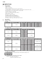
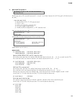
(2) Fs=39.69 kHz (44.1 kHz-10 %)
· Set the oscillator to 39.69 kHz.
· Make the same input as 2-4 1 and confirm that the same output level is attained. Or, conduct a listening test for one minute
to check that there is no noise.
3.
Sound
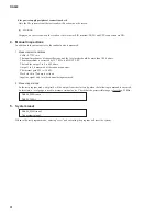
Perform a listening test to confirm the following items.
· OUTPUT
4.
Settings after inspection
· Internal gain SW:
+18 dB
· WORD CLOCK IN 75 ohms:
ON
WORD CLOCK (AD824)
Input frequency
Input frequency
Even channels are also the same.
Output level (Odd CH)
Permissible range (Even CH)
+16 dBu
Less than -54 dBu
1 kHz
(6) Maximum output
Conditions: Inspect the cannon connector and phone connector individually.
Output level
Permissible range
+18 dBu
+18
±
0.5 dBu
Permissible range (Distortion ratio)
Less than 0.01 %
1 kHz
2-2
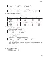
Operation confirmation of level meters 1 to 8
Conditions:
Input specified level to AD824 input 1 to 8.
AD824 can also have simultaneous input of channels 1 to 8
Visually confirm the on and off of the peak, nominal and signal LEDs.
(1) On (Lit)
LED level
Input frequency
Input level (AD824)
Permissible range
Reference output level
PEAK
NOMINAL
SIGNAL
1 kHz
1 kHz
1 kHz
+21 dBu
+10 dBu
-10 dBu
0 – +2 dB
0 – +2 dB
0 – +2 dB
+15 dBu
+4 dBu
-16 dBu
(2) Off (Not lit)
LED level
Input frequency
Input level (AD824)
Permissible range
Reference output level
PEAK
NOMINAL
SIGNAL
1 kHz
1 kHz
1 kHz
+18 dBu
+8 dBu
-12 dBu
0 dB
0 dB
0 dB
+12 dBu
+2 dBu
-18 dBu
2-3
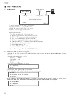
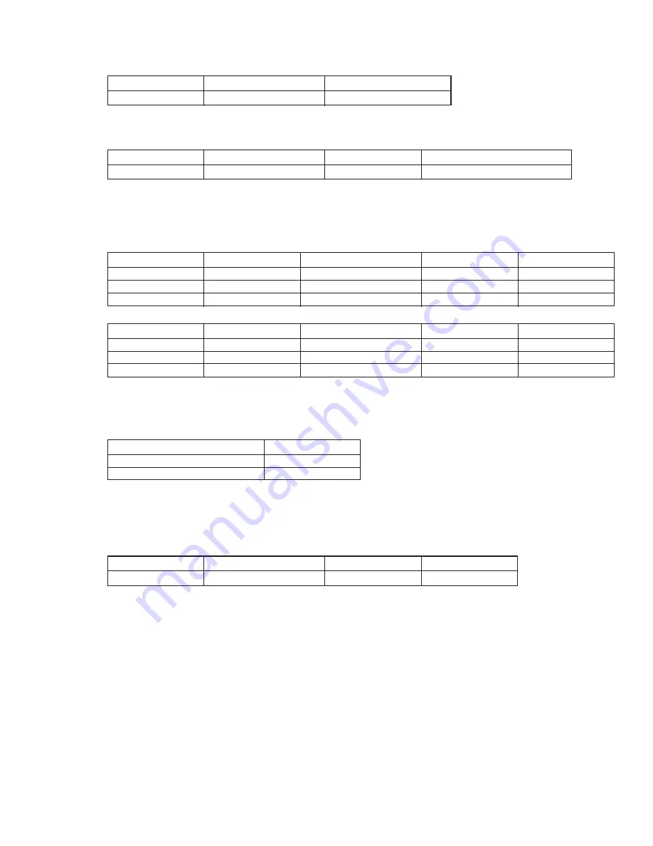
Jitter measurement
· Connect AD824 word clock out and DA824 word clock in.
· Insert MY8-AE card into the slot and connect to DSA1 via the D-sub-cannon converter box.
· Set AD824 word clock settings to 48 kHz and 44.1 kHz.
Permissible range
48 kHz
44.1 kHz
Less than 6 nsec
Less than 5 nsec
2-4
Fs operating range
· Connect the oscillator to AD824 word clock in.
(1) Fs=50.88 kHz (48 kHz+6 %)
· Set the oscillator to 50.88 kHz.
· Conduct a listening test for one minute to check that there is no noise.
Input frequency
Input level (AD824)
Output level
Permissible range
1 kHz
+10 dBu
+4 dBu
+4
±
1 dBu
Summary of Contents for DA824
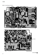
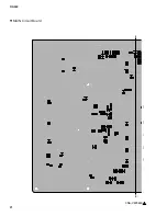
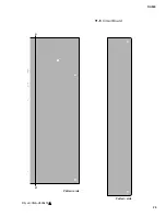
Page 21: ...E E 3NA V485480 1 DA824 21 MAIN Circuit Board ...
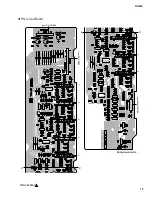
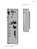
Page 22: ...E E MAIN MYSL 3NA V485480 1 MYSL Circuit Board Pattern side Pattern side DA824 22 ...
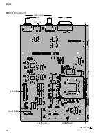
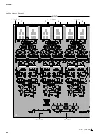
Page 25: ...3NA V485470 1 G G DA Circuit Board DA824 25 ...
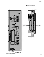
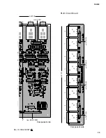
Page 26: ...DA JK 3NA V485470 1 G G JK Circuit Board Pattern side Pattern side DA824 26 ...


