background image

DTXTREME

90

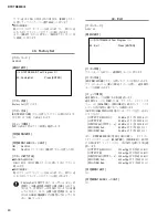
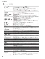
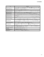
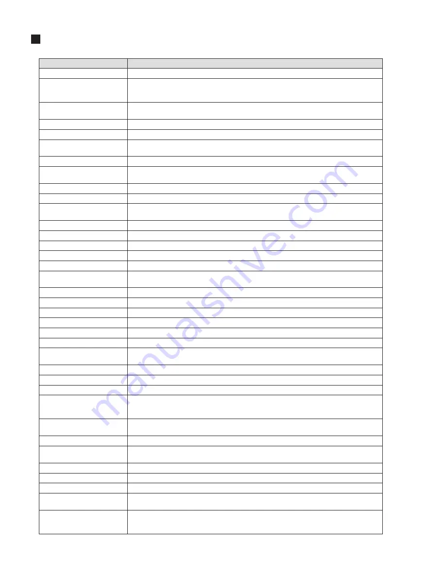
 DISPLAY MESSAGES

Ad

i

LCD

Description

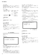
Are you sure? 

Con

fi

rms whether you want to execute a speci

fi

ed operation or not.

Can’t play SMF Format 1 data.

This message appears when you select and start the song with the SMF format 1 on the USB storage
device. Convert the song to the SMF format 0, then play it again, since the DTXTREME

 can handle 

only SMF format 0 song data.

Choose user song.

This message appears when you press the [F2] JOB button in the Song mode with a Preset Song 
selected. When you want to call up the Job display, select a User Song.

Click stored.

The settings in the Click mode have been stored.

Completed.

This appears when an operation such as Load, Save, Format and other Job has been completed.

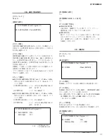
Connecting USB device...

The DTXTREME

is currently recognizing the USB storage device connected to the USB TO DEVICE

terminal.

Copy protected.

You have attempted to export or save a copy-protected digital audio source.

USB device full.

The USB storage device is full and no more data can be saved. Use a new USB storage device, or 
make space by erasing unwanted data from the storage device.

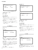
USB device not ready.

A USB storage device is not properly inserted in or connected to the DTXTREME

.

USB device read/write error.

An error occurred while reading or writing to/from a USB storage device.

USB device write protected.

A USB storage device is write protected, or you have attempted to write to a read-only medium such as
CD-ROM.

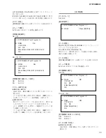
Executing...

A format operation or Job is being executed.

File already exists.

fi

le having the same name as the one you are about to save already exists.

File not found.

The speci

fi

ed 

fi

le was not found on the external USB storage device during a Load operation.

Folder is not empty.

You have attempted to delete a folder that contains data.

Folder is too deep.

Directories below this level cannot be accessed.

Illegal file.

The 

fi

le speci

fi

ed for loading is unusable by the DTXTREME

 or cannot be loaded in the current 

mode.

Illegal file name.

The speci

fi

ed 

fi

le name is invalid. Try entering a different name.

Illegal input.

An invalid input or value has been speci

fi

ed. Check the input method or value.

Illegal sample data.

The sample 

fi

le speci

fi

ed for loading is unusable by the DTXTREME

.

Illegal selection.

An unacceptable 

fi

le has been speci

fi

ed in the Song job mode.

Illegal song number.

An unacceptable song number has been speci

fi

ed in the Song job mode. Select the song again.

Illegal track number.

An unacceptable track number has been speci

fi

ed in the Song job mode. Select the track again.

Incompatible USB device.

A USB device which cannot be used with the DTXTREME

 has been connected to the USB TO

DEVICE connector.

Invalid USB device.

The USB storage device is unusable. Format the USB storage device and try again.

MIDI buffer full.

Failed to process the MIDI data because too much data was received at one time.

MIDI data error.

An error occurred when receiving MIDI data.

No data.

When a Song Job was executed, the selected track or range contained no data. Select an appropriate
track or range. In addition, this message appears when a Job related to a Mixing Voice cannot be exe-
cuted because the speci

fi

ed Mixing Voice is not available.

No DIMM memory installed.

An appropriate pair of expansion DIMMs has not been properly installed, or the pair is not properly
matched.

No response from USB device.

There is no response from the USB device connected to the USB TO DEVICE terminal.

No sample data.

This message appears when a Sample-related Job cannot be executed because the speci

fi

ed Sample

is not available.

Now loading... (xxxx) 

Indicates that a 

fi

le is being loaded.

Now saving... (xxxx) 

Indicates that a 

fi

le is being saved.

Now scanning autoloaded files.

The DTXTREME

 is currently scanning for the 

fi

les speci

fi

ed for Auto Load.

Now working...

The DTXTREME

 is currently executing the memory arrangement after you have 

fi

nished Sampling 

or have cancelled the Load/Save operation by pressing the [EXIT] button.

Overwrite? [YES]/[NO] 

This message appears when the Save operation in the File mode will overwrite data on the USB stor-
age device or the Sampling operation will overwrite the User Voice containing data. This message 
prompts you to con

fi

rm whether it is OK to continue the operation or not.

Summary of Contents for DTXTREME III

Page 1: ...LLATION DIMM 拡張メモリー の取り付け 16 LSI PIN DESCRIPTION LSI 端子機能表 21 IC BLOCK DIAGRAM IC ブロック図 25 CIRCUIT BOARDS シート基板図 27 TEST PROGRAM テストプログラム 44 63 DEFAULT SETTING 出荷時の設定 82 SAVING and LOADING A FILE ファイルのセーブ ロード 83 CONTENTS 目次 INITIAL FACTORY SETTING ファクトリーセット 85 VERSION UPDATE バージョンアップ 87 MEMORY STRUCTURE メモリー構成 88 89 DISPLAY MESSAGES メッセージリスト 90 92 BOOT SEQUENCE 起動シーケンス 94 95 MIDI IMPLEMENTATION CH...

Page 2: ...sale of this manual to any individual or firm does not constitute authorization certification recognition of any applicable technical capabilities or establish a principal agent relationship of any form The data provided is belived to be accurate and applicable to the unit s indicated on the cover The research engineering and service departments of Yamaha are continually striving to improve Yamaha...

Page 3: ...signals via OUTPUT Resample Sample Data Bits 16bit Sampling Frequency 44 1kHz 22 05 kHz 11 025 kHz 5 5125 kHz stereo mono Sampling Memory Optionally installed expandable to 512 MB 256 MB DIMM x 2 slots DIMMs are not installed to the instrument when shipped from the factory Sample Length Mono 32MB Stereo 64MB Sampling Time 44 1kHz 6 min 20 sec 22 05kHz 12 min 40 sec 11 025kHz 25 min 20 sec 5 5125kH...

Page 4: ...ナログ入力L R ステレオアウト リサンプリング サンプルデータビット 16 bit サンプリング周波数 44 1 kHz 22 05 kHz 11 025 kHz 5 5125 kHz ステレオ モノ 波形メモリー 最大拡張時512 MB 256 MB DIMM x2 工場出荷時にはDIMMは装着されていません 最大サンプルサイズ 1モノサンプル 32 MB 1ステレオサンプル 64 MB 1回あたりのサンプリング時間 44 1 kHz 約6分20秒 22 05 kHz 約12分40秒 11 025 kHz 約25分20秒 5 5125 kHz 約55分40秒 ステレオ モノいずれの場合でも同様 サンプルフォーマット DTXTREMEⅢオリジナルフォーマット WAV AIFF その他 操作子 スライダーボリューム MASTER PHONES CLICK ACCOMP KICK SNARE...

Page 5: ... HI HAT slider 5 MISC slider 6 Data dial 7 DEC NO button 8 INC YES button 9 Cursor buttons 0 EXIT button 1 ENTER STORE button q LCD 液晶ディスプレイ w LED ディスプレイ e DRUM KIT ドラムキット ボタン r CLICK クリック ボタン t FILE ファイル ボタン y CHAIN チェーン ボタン u SONG ソング ボタン i TRIGGER トリガー ボタン o UTILITY ユーティリティ ボタン 0 SAMPLING サンプリング ボタン 1 TRIGGER INDICATOR トリガーインジケーター 2 Audition オーディション ボタン 3 F1 F6 ファンクショ ン ボタン 4 SF1 SF6 サブファ ンクション...

Page 6: ... DEVICE and USB TO HOST terminals 3 HI HAT CONTROL jack 4 Trigger Input jack qSNARE oHI HAT 5 Trigger Input jack 0 1 KICK 6 Trigger Input jack 2 5 q STANDBY ON スタンバイ オン スイッチ w DC IN 端子 e コードフック r LCD CONTRAST LCD コントラスト ノブ t GAIN ノブ y AUX IN SAMPLING IN 端子 u OUTPUT L MONO OUTPUT R 端子 i PHONES ヘッドフォン 端子 o INDIVIDUAL OUTPUT 1 6 端子 0 DIGITAL OUT 端子 1 MIDI IN OUT 端子 2 USB TO DEVICE USB TO HOST 端子 3 HI...

Page 7: ...TXTREMEⅢ Standard Set スタンダードセット Referring to the illustration below or next page connect the output cable from each pad to each Trigger Input jack located on the rear panel of the DTXTREMEⅢ All Trigger Input jacks are conveniently labeled qSNARE etc so make sure each pad is connected to its corresponding Trigger Input jack WARNING To prevent electric shock and damage to the devi ces make sure the ...

Page 8: ...K to SNARE Foot pedal is not included in the Special Set フットペダルはスペシャル セットには含まれません Holder モジュールホルダー included 付属品 Wing Bolt ちょうボルト x 4 included 付属品 DTXTREMEⅢ Attaching the holder Attach the included holder to the DTXTREMEⅢ using the wing bolts Be sure to use the included screws DTXTREMEⅢの取り付け DTXTREMEⅢに付属のモジュールホルダーとちょうボルトを使って 左図のように取り付けます 必ず付属の止めネジを使用してください DTXTREMEⅢ Special Set スペシャルセット ...

Page 9: ...9 DTXTREMEⅢ CIRCUIT BOARD LAYOUT ユニットレイアウト JK DM PN DMSUB Bottom view Bottom view Bottom view Bottom view Display assembly ディスプレイ Ass y DM PN DMSUB Optional DIMM 拡張メモリー ...

Page 10: ...H 3 0X8 MFZN2B3 WE975300 Fig 1 図 1 400 400 400 400 400 Side cover L サイドカバー L Side cover R サイドカバーR Notes on Flat Cable Contacts are visible through the back side When connecting to the connector pay attention not to insert the cable inversely Photo A During assembly pay attention that connectors cables or the like are not pinched by circuit boards frames etc フラットケーブルの注意 接点が裏面から透けて見えます コネクタにケーブル の表 ...

Page 11: ...cedure 1 2 2 Remove the following screws and remove the bot tom case Fig 2 410A 18pcs 2 ボトムケース 所要時間 約 5 分 2 1 サイドカバー L R を外します 1 項参照 2 2 下記のネジを外して ボトムケースを外します 図 2 410A 18 本 410A Bind Head Tapping Screw B B タイト BIND 3 0X8 MFZN2W3 WE774300 Fig 2 図 2 Bottom view 底から見た図 Bottom case ボトムケース 410A 410A 410A ...

Page 12: ...ure 1 3 2 Remove the bottom case See procedure 2 3 3 Remove the following screws and remove the JK circuit board from the PCB locking spacer Fig 3 390A 6pcs PCB Locking Spacer 2pcs Remove the head portion from the hole of the JK circuit board while holding the head portion with pliers or the like 3 JK シート 所要時間 約 6 分 3 1 サイドカバー L R を外します 1 項参照 3 2 ボトムケースを外します 2 項参照 3 3 下記のネジを外して ロッキングスペーサから JK シートを...

Page 13: ...the whole internal setup data on a USB memory See page 83 When the connector assembly is disconnected from the connector CN18 the protection sheet will be disconnected as well Take care not to lose the protection sheet 5 DM シート 所要時間 約 9 分 5 1 サイドカバー L R を外します 1 項参照 5 2 ボトムケースを外します 2 項参照 5 3 JK シートを外します 3 項参照 5 4 DMSUB シートを外します 4 項参照 5 5 下記のネジを外して DM シートを外します 図 5 410D 6 本 拡張メモリー オプション は DM シートの構成 部...

Page 14: ...ollowing screws and remove the PN angle F Fig 7 410F 3pcs 6 9 Remove the following screws and remove the PN circuit board Fig 8 390C 3pcs 410G 5pcs 6 PN シート 所要時間 約 12 分 6 1 コントロールパネル面よりエンコーダツマミ S を抜いておきます 図 6 6 2 サイドカバー L R を外します 1 項参照 6 3 ボトムケースを外します 2 項参照 6 4 JK シートを外します 3 項参照 6 5 DMSUB シートを外します 4 項参照 6 6 DM シートを外します 5 項参照 6 7 下記のネジを外して PN アングル R を外します 図 7 410E 3 本 6 8 下記のネジを外して PN アングル F を外します ...

Page 15: ...See procedure 6 7 7 Remove the following screws and remove the dis play assembly Fig 8 410H 4pcs 7 ディスプレイ Ass y 所要時間 約 11 分 7 1 サイドカバー L R を外します 1 項参照 7 2 ボトムケースを外します 2 項参照 7 3 JK シートを外します 3 項参照 7 4 DMSUB シートを外します 4 項参照 7 5 DM シートを外します 5 項参照 7 6 PN シートを外します 6 項参照 7 7 下記のネジを外して ディスプレイ Ass y を外し ます 図 8 410H 4 本 390C Bind Head Tapping Screw B B タイト BIND 3 0X10 MFZN2B3 WE972200 410G 410H Bind Head Tap...

Page 16: ... mayalso result in poor electrical contact or electrostatic damage Be careful of static electricity Static electricity discharge can damage the IC chips on the DIMM Before you handle the optional DIMM to reduce the possibility of static electricity touch unpainted metal parts or a ground wire on the devices that are grounded Handle the optical units with care Dropping or subjecting them to any kin...

Page 17: ... module and leave the second memory socket open Also make sure each DIMM in the pair is of the same manufac turer and the same type DIMMs of different makers and configurations may not work together When purchasing DIMMs make sure that the DIMM design does not utilize more than 18 memory chips per module DIMMs comprised of more than 18 chips do not operate correctly on the DTXTREME Ⅲ 64MB x 2 128M...

Page 18: ...al and Sliders 3 Remove the slot cover Remove the screws from the slot cover by using a Phillips screw driver Rear panel リアパネル面 Bottom surface of the DTXTREMEⅢ DTXTREMEⅢ 底面 重要 外したネジはなくさないようにしてください このネジは DIMM取り付け後 再度使用します Slot cover スロットカバー Underside of the DTXTREMEⅢ DTXTREMEⅢ底面 IMPORTANT Keep the removed screws in a safe place They will be used when re attaching the cover to the instrument after i...

Page 19: ...を確かめて取り付けてください Ejector lever ロックレバー Notch for alignment 切り欠き 4 1 Press the ejector levers to the outside of the socket 4 2 Insert the DIMM vertically in the socket Press the DIMM in firmly until it snaps or locks in place Confirm whether or not both the levers are firmly locked 4 DIMM を 2 枚 DIMM スロットに垂直に奥まで差し 込みます DIMM スロットへの取り付け 4 1 左右のロックレバーを横に押して 倒します 4 2 DIMM を垂直に 奥まで差し込みます 同時にレバーが立ち上げられ DIMM ...

Page 20: ...cated in the display Memory size メモリー容量 If the DIMMs have not been installed properly the Sampling function will not work correctly If this occurs turn the power off perform the instructions above again and make sure to install the DIMMs firmly Removing DIMMs 1 Press the ejector lever until the DIMM unlocks 2 Pull the DIMM vertically out of the socket 5手順 3 で取り外したスロットカバーを 逆の手順で取 り付けます スロットカバーを取り付け...

Page 21: ... WR P66 WAIT P67 ASTB P40 AD0 P41 AD1 P42 AD2 P43 AD3 P44 AD4 P45 AD5 P46 AD6 A47 AD7 I I I I I I O I O I O I O I O I O I O I O I O I O I O I O I O I O I O I O I O I O I O I O I O I O Port 1 A D converter analog input A D converter reference voltage input Analog power supply 5 V System reset input Subsystem clock oscillation Internally connected Main system clock oscillation Ground Port 0 External...

Page 22: ...24 125 126 127 128 129 130 131 132 133 134 135 136 137 138 139 140 141 142 143 144 145 146 147 148 149 150 151 152 153 154 155 156 157 158 159 160 161 162 163 164 165 166 167 168 169 170 171 172 173 174 175 176 177 178 179 180 181 182 183 184 185 186 187 188 189 190 191 192 193 194 195 196 197 198 199 200 201 202 203 204 205 206 207 208 209 210 E22 D23 C24 B25 A26 E23 F22 D24 C25 B26 C26 F23 G22 E...

Page 23: ...351 352 353 354 355 356 357 358 359 360 361 362 363 364 365 366 367 368 369 370 371 372 373 374 375 376 377 378 379 380 381 382 383 384 385 386 387 388 389 390 391 392 393 394 395 396 397 398 399 400 401 402 403 404 405 406 407 408 409 410 411 412 413 414 415 416 417 418 419 420 AB22 AC23 AD24 AE25 AF26 AC22 AB21 AD23 AE24 AF25 AF24 AC21 AB20 AD22 AE23 AF23 AC20 AD21 AB19 AC19 AE22 AF22 AD20 AE21 ...

Page 24: ...PTJ 0 Reserved PTJ 1 Reserved CAS PTJ 2 VssQ Reserved PTJ 3 VccQ Reserved PTJ 4 Reserved PTJ 5 Vss PTD 5 CL1 Vcc PTD 7 DON PTE 6 M_DISP PTE 3 FLM PTE 0 TDO PCC0RESET DRACK0 PCC0DRV_ DACK0_ WAIT RESETM ADTRG PTH 5 IOIS16 PTG 7 ASEMD0 PTG 5 ASEBRKAK_ PTG 4 PCC0BVD2 PTG 3 AUDATA 3 PCC0BVD1 PTG 2 AUDATA 2 Vss PCC0CD2 PTG 1 AUDATA 1 Vcc PCC0CD1 PTG 0 AUDATA 0 VssQ PTF 7 PINT 15 TRST_ VccQ PTF 6 PINT 14...

Page 25: ... output Lch negative analog output Lch positive analog output Common voltage output Parallel serial select Master clock select DMSUB IC116 118 PN IC706 707 IC BLOCK DIAGRAM IC ブロック図 SN74AHCT125PWR X4152A00 DM IC13 Quad 3 State Bus Buffer 1 2 3 4 5 6 7 C1 A1 Y1 C2 A2 Y2 GND 14 13 12 11 10 9 8 Vcc C4 A4 Y4 C3 A3 Y3 TC74VHC08F XT014B00 DM IC18 Quad 2 Input AND 1 2 3 1A 1Y 4 2A 5 2B 6 2Y 7 VSS 1B 14 1...

Page 26: ...04M XV190A00 JK IC301 306 321 324 329 333 335 337 Dual Operational Amplifier 1 2 3 4 8 7 6 5 Output A V Non Inverting Input A Ground DC Voltage Supply Output B Inverting Input B Non Inverting Input B Inverting Input A NJM2114M TE1 XS537B00 DMSUB IC105 107 PN IC710 Dual Operational Amplifier 1 2 3 4 8 7 6 5 A Output V A Input V V B Output B Input B Input A Input HD74LVC139FPEL XS048A00 DM IC23 Dual...

Page 27: ...Active low open drain output Indicates overcurrent UVLO and thermal shutdown Ground Not internally connected Supply Input Input to the power switch and the supply voltage for the IC Switch Output Output of the high side switch Pins 6 and 8 must be tied together LTC1144CS8 X9457A00 DMSUB IC127 Voltage Converter 12V 1 2 3 4 8 7 6 5 BOOST CAP CAP GND V VOUT OSC SHDN Pin No 1 2 3 4 6 5 7 8 Pin Name BO...

Page 28: ...to DMSUB CN107 to DMSUB CN104 to DMSUB CN103 to JK CN301 to DMSUB CN102 to DMSUB CN113 to DMSUB CN111 to DMS not installed not installed not installed not installed not installed not installed A A DM Circuit Board 2NA WJ91030 1 ...

Page 29: ...29 DTXTREMEⅢ to DMSUB CN110 to DMSUB CN101 DIMM socket DIMM socket to PN CN701 not installed not installed not installed not installed A A Component side 部品側 2NA WJ91030 1 ...

Page 30: ...DTXTREMEⅢ 30 B B DM Circuit Board 2NA WJ91030 2 ...

Page 31: ...31 DTXTREMEⅢ B B Pattern side パターン側 2NA WJ91030 2 ...

Page 32: ...DTXTREMEⅢ 32 to DM CN18 to DM CN12 to PN CN702 to DM CN6 STANDBY ON DIGITAL OUT 4 0 1 6 INDIVIDUAL OUTPUT DC IN 16V C C DMSUB Circuit Board 2NA WJ91040 ...

Page 33: ...DTXTREMEⅢ to DM CN5 to DM CN14 to DM CN15 to DM CN1 to PN CN706 to PN CN702 to DM CN6 to JK CN302 to DM CN11 DIGITAL OUT OUT IN 4 USB MIDI TO HOST TO DEVICE C C Component side 部品側 Scale 85 100 2NA WJ91040 ...

Page 34: ...DTXTREMEⅢ 34 D D DMSUB Circuit Board 2NA WJ91040 ...

Page 35: ...35 DTXTREMEⅢ D D Pattern side パターン側 Scale 85 100 2NA WJ91040 ...

Page 36: ...DTXTREMEⅢ 36 to DM CN13 to PN CN707 to DMSUB CN109 SNARE 4 TOM1 TOM2 0 TOM3 1 TOM4 6 RIDE 2 CRASH1 CRASH2 HI HAT E E JK Circuit Board 2NA WJ91050 1 ...

Page 37: ...37 DTXTREMEⅢ CRASH2 HI HAT KICK HI HAT CONTROL E E Component side 部品側 Scale 95 100 2NA WJ91050 1 ...

Page 38: ...DTXTREMEⅢ 38 F F JK Circuit Board 2NA WJ91050 2 ...

Page 39: ...39 DTXTREMEⅢ F F Pattern side パターン側 Scale 95 100 2NA WJ91050 2 ...

Page 40: ...MSUB CN108 G G ENTER STORE PN Circuit Board 2NA WJ91060 1 SW720 F3 SW721 SF3 SW722 F4 SW723 SF4 SW724 F5 SW725 SF5 SW726 F6 SW727 SF6 SW728 DEC ON SW729 SW730 EXIT SW731 SW732 SW733 INC YES SW734 SW735 ENTER EC701 1 DEC 1 INC VR703 KICK VR704 SNARE VR705 TOM VR706 CYMBAL VR707 HI HAT VR708 MISC ...

Page 41: ...CLICK SW703 LD703 FILE SW704 LD704 CHAIN SW705 LD705 SONG SW706 LD706 TRIGGER SW707 LD707 UTILITY SW708 LD708 SAMPLIMG SW709 w SW710 LD711 REC SW711 1 SW712 LD710 SW713 SW714 LD712 CLICK ON OFF SW715 LD713 TRIGGER INDICATOR SW16 F1 SW17 SF1 SW18 F2 SW19 SF2 VR711 MASTER VR710 PHONES VR701 CLICK VR702 ACCOMP C and have different hole diameters Printing on the surface and patterns are identical C と ...

Page 42: ...DTXTREMEⅢ 42 H H or D PN Circuit Board 2NA WJ91060 2 ...

Page 43: ...43 DTXTREMEⅢ H H Pattern side パターン側 Scale 80 100 2NA WJ91060 2 ...

Page 44: ...k the operation of the pad encoder A0 16 00 23 HiHat Check the operation of the hi hat controller A0 17 00 24 MIDI Check the operation of the MIDI IN OUT 25 USB ToDevice Check the operation of the USB TO DEVICE A0 19 00 26 USB ToHost Check the operation of the USB TO DEVICE TO HOST A0 1A 00 27 OUTPUT L Check the output signal of the OUTPUT L MONO and DIGITAL OUT A0 1B 00 28 OUTPUT R Check the outp...

Page 45: ...rogram Firm Ver Kernel Ver ATT min 36 max 41 CR min 0c max 18 XT 02 ENTER Test Start F6 Factory Set Data Ver EXIT Exit Version number DTXTREME III Test Program Firm Ver Kernel Ver ATT min 36 max 41 CR min 0c max 18 XT 02 Wating test code Data Ver EXIT Exit Version number Press the F6 button to execute the Factory Set See 43 Factory set on page 61 Press the EXIT button to finish the test mode follo...

Page 46: ...ectly Test method Connect the headphones Set the PHONES slider of the DTXTREMEⅢ to a little hi gher position Adjust the volume as necessary Press the ENTER STORE button to execute the test Check item Turn on the panel switches the DRUM KIT ENTER STORE in the order shown on the LCD Check also that the LED will light if a button with an LED is pressed Press the CLICK ON OFF switch twice to check tha...

Page 47: ...s the ENTER STORE button to execute the test auto matically LEDs will light in turn in the following order DTXTREME III Test Program 03 7SEG LED Press ENTER Check item Check that LEDs light in the order shown in the above figure Check visually that no LED lights too dimly too Judgment indication In case of OK None In case of NG None MIDI code output for judgment result None How to quit test MANUAL...

Page 48: ...ncoder 8 0 MIDI MODE Send a test code for another test to stop the current test and the test for the newly sent test code will be executed Press the EXIT button to return to the MIDI test code standby screen 05 Slider Test Code A0 05 00 Initial indication DTXTREME III Test Program 04 Encoder OK Test contents Move the slider slide volume and check for operation Test method Press the ENTER STORE but...

Page 49: ...ewly sent test code will be executed Press the EXIT button to return to the MIDI test code standby screen 07 Trigger In1 08 Trigger In2 09 Trigger In3 10 Trigger In4 11 Trigger In5 12 Trigger In6 13 Trigger In7 14 Trigger In8 15 Trigger In9 16 Trigger In10 17 Trigger In11 18 Trigger In12 19 Trigger In13 20 Trigger In14 21 Trigger In15 Test Code DTXTREME III Test Program 06 Rim SW Press ENTER DTXTR...

Page 50: ...I HAT 0KICK 1 Lch 0KICK 1 Rch 2 3 4 5 Check item Check the test result indicated on the LCD Judgment indication In case of OK example of test 07 DTXTREME III Test Program 07 Trigger In1 OK In case of NG example of test 07 DTXTREME III Test Program 07 Trigger In1 NG Xtalk IN 2 29 too Hi NG due to too large input level Xtalk IN NG due to signal leak of to the channel BAD Curve NG due to waveform att...

Page 51: ...ad Encoder OK In case of NG Example qSNARE is NG DTXTREME III Test Program 22 Pad Encoder PadEnc 1 NG PadEnc 4 8 WAIT PadEnc 2 8 WAIT PadEnc 5 8 WAIT PadEnc 3 8 WAIT In case of NG If any input is NG DTXTREME III Test Program 22 Pad Encoder NG MIDI code output for judgment result OK A0 16 02 NG A0 16 03 How to quit test MANUAL MODE In case of OK press the INC YES button to proceed to the next test ...

Page 52: ...before starting the test Press the ENTER STORE button to execute the test Check item Check the test result indicated on the LCD Judgment indication In case of OK DTXTREME III Test Program 24 MIDI Press ENTER In case of NG TIME OUT failure DTXTREME III Test Program 24 MIDI OK In case of NG other failure DTXTREME III Test Program 24 MIDI NG TIME OUT MIDI code output for judgment result None How to q...

Page 53: ...t test If the test is aborted with the judgment of NG press the EXIT button to return to the Test number selection screen MIDI MODE Send a test code for another test to stop the current test and the test for the newly sent test code will be executed Press the EXIT button to return to the MIDI test code standby screen 26 USB ToHost Test Code A0 1A 00 Initial indication Test contents Execute a loopb...
Page 54: ...sure frequency waveform level and distortion of each output After the measurement disconnect the plug connected to the OUTPUT R jack and measure the output from the OUTPUT L MONO then Insert standard stereo plug to the PHONES jack and measure frequency waveform level and distortion of each output Check also that sound is outputted from the DIGITAL OUT jack Do not insert a plug to the AUX IN SAMPLI...

Page 55: ...NDIVIDUAL OUTPUT 1 6 jacks and measure frequency waveform level and distortion of each output Check item INDIVIDUAL OUTPUT 1 3 5 Frequency 1 kHz 1 5 Hz Waveform Sine wave Level 4 0 2 dBu load of 10 kΩ Distortion 0 1 or less INDIVIDUAL OUTPUT 2 4 6 Level 88 dBu or less load of 10 kΩ Judgment indication None Test contents Check that specified signals are outputted from the OUTPUT and PHONES jacks Te...

Page 56: ...are outputted from the INDI VIDUAL OUTPUT 2 4 6 jacks Check the crosstalk value at the INDIVIDUAL OUTPUT 1 3 5 jacks Test method Press the ENTER STORE button to execute the test Insert standard phone plugs to the INDIVIDUAL OUTPUT 1 6 jacks and measure frequency waveform level and distortion of each output Check item INDIVIDUAL OUTPUT 2 4 6 Frequency 1 kHz 1 5 Hz Waveform Sine wave Level 4 0 2 dBu...

Page 57: ...em Input sine wave of 52 dBu 1 kHz with distortion of 0 1 or less to the Lch of the AUX IN SAMPLING IN jack Connect the Rch to the GND OUTPUT L MONO Level 2 0 2 dBu load of 10 kΩ Distortion 0 5 or less OUTPUT R Level 65 0 dBuor less DTXTREME III Test Program 37 AUX IN MIC Press ENTER Input sine wave of 52 dBu 1 kHz with distortion of 0 1 or less to the Rch of the AUX IN SAMPLING IN jack Connect th...

Page 58: ...ess to the DIMM works normally Test method Check that the DIMM is inserted and press the ENTER STORE button to execute the test If the DIMM is not inserted be sure to turn off the power to the DTXTREMEⅢ before inserting the DIMM See pages 16 20 Check item Check the test result indicated on the LCD Check that the memory size of the DIMM is indicated normally Judgment indication In case of OK DTXTRE...

Page 59: ...n In case of OK In case of NG DTXTREME III Test Program 40 DIMM Full Press ENTER MIDI code output for judgment result OK A0 28 02 NG A0 28 03 How to quit test MANUAL MODE In case of OK press the INC YES button to proceed to the next test If the test is aborted with the judgment of NG press the EXIT button to return to the Test number selection screen MIDI MODE Send a test code for another test to ...

Page 60: ...pared with the written data Test method Press the ENTER STORE button to execute the test Check item Check the test result indicated on the LCD Judgment indication In case of OK DTXTREME III Test Program 41 ROM OK IC 33 IC 32 OK OK Wave Rom IC 36 IC 37 IC 39 IC 40 OK In case of NG Example DTXTREME III Test Program 41 ROM NG IC 33 IC 32 OK OK Wave Rom IC 36 IC 37 IC 39 IC 40 NG MIDI code output for ...

Page 61: ...mode and resets to the normal operation mode Test method Press the ENTER STORE button to execute the test Press the INC YES button in the test mode to start the normal operation mode Check item Check that the normal operation mode starts After the normal operation mode is started turn the sliders slide volumes MASTER and PHONES to the maximum and check the noise level meets the following requireme...

Page 62: ...I If you want to select USB press the INC YES button t Press the ENTER STORE button to enter the setting SF3 UTILITY ENTER STORE Front Panel EXIT DEC NO F5 q w e 2 In case test codes transmitted through the MIDI jack are not accepted Test codes are not accepted during the following tests Stop the test during execution by pressing the EXIT button and transmit a test code again 02 Panel SW 04 Encode...

Page 63: ...5 Lch の入力レベル等を確認します A0 15 00 22 Pad Encoder ドラムパッドのパッドエンコーダ動作を確認します A0 16 00 23 HiHat ドラムパッドのハイハットコントローラ動作を確認します A0 17 00 24 MIDI MIDI IN OUT の動作を確認します 25 USB ToDevice USB TO DEVICE の動作を確認します A0 19 00 26 USB ToHost USB TO DEVICE TO HOST の動作を確認します A0 1A 00 27 OUTPUT L OUTPUT L MONO DIGITAL OUT の出力信号を確認します A0 1B 00 28 OUTPUT R OUTPUT R の出力信号を確認します A0 1C 00 29 INDIV 1 3 5 INDIVIDUAL OUTPUT 1 3 5 の出力信...

Page 64: ...E III Test Program Firm Ver Kernel Ver ATT min 36 max 41 CR min 0c max 18 XT 02 ENTER Test Start F6 Factory Set Data Ver EXIT Exit バージョン番号 DTXTREME III Test Program Firm Ver Kernel Ver ATT min 36 max 41 CR min 0c max 18 XT 02 Wating test code Data Ver EXIT Exit バージョン番号 EXIT ボタンを押すと テストモードを終了し 通 常動作モードに入ります 44 Exit 80 ページ 参照 MIDI MODE DTXTREMEⅢの電源立ちあげ後 数秒待ち プレイ画 面の表示になったことを確かめた後 F0 43 10 18 5A 00 F...

Page 65: ...ンを押して テス トナンバー選択画面 に戻り 次のテストに進みます MIDI MODE 他のテストのテストコードを送ると終了し 新たに送 られてきたテストコードのテストが実行されます また EXIT ボタンを押すと MIDI テストコード待 ち画面 に戻ります 02 Panel SW テストコード A0 02 00 最初の表示 テスト内容 パネルスイッチが正しく動作する事を確認します テスト方法 ヘッドフォンを接続します DTXTREMEⅢの PHONES スライダーを少し上げます 音量は適宜調整してください ENTER STORE ボタンを押して テストを実行させます チェック項目 DRUM KIT から ENTER STORE までのパネルスイッ チを LCD の表示に従って以下の順に ON します LED 表示のあるボタンは 押した時に LED が点灯する 事も確認します CLICK...

Page 66: ...ストナンバー選択画面 に戻ります MIDI MODE 他のテストのテストコードを送ると終了し 新たに送 られてきたテストコードのテストが実行されます また EXIT ボタンを押すと MIDI テストコード待 ち画面 に戻ります 03 7SEG LED テストコード A0 03 00 最初の表示 DTXTREME III Test Program 03 7SEG LED Press ENTER テスト内容 7SEG LED の点灯が正常に動作する事を確認します 各 LED が点灯した時 PHONES OUTPUT 端子か ら SIN 波が出力されます テスト方法 ヘッドフォンを接続します DTXTREMEⅢの PHONES スライダーを少し上げます 音量は適宜調整してください ENTER STORE ボタンを押せば 自動的にテストが実 行されます 下記の順番で 対応する LED が順次点灯し...

Page 67: ...der 8 0 DTXTREME III Test Program 04 Encoder 8 0 判定結果の表示 OK の時 DTXTREME III Test Program 04 Encoder OK NG の時 なし 判定結果の MIDI コード出力 OK A0 04 02 NG なし テストの終了方法 MANUAL MODE OK の時は INC YES ボタンを押して次のテストに 進みます MIDI MODE 他のテストのテストコードを送ると終了し 新たに送 られてきたテストコードのテストが実行されます また EXIT ボタンを押すと MIDI テストコード待 ち画面 に戻ります 05 Slider テストコード A0 05 00 最初の表示 DTXTREME III Test Program 05 Slider Press ENTER テスト内容 スライダー スライドボリューム...

Page 68: ... られてきたテストコードのテストが実行されます また EXIT ボタンを押すと MIDI テストコード待 ち画面 に戻ります 06 Rim SW テストコード A0 06 00 最初の表示 DTXTREME III Test Program 06 Rim SW Press ENTER テスト内容 ドラムパッドのリムスイッチが 正常に動作する事を確 認します テスト方法 ENTER STORE ボタンを押して テストを実行させます qSNARE oHI HAT 2 5 の各チャンネル に リムスイッチ付き 3 ゾーンドラムパッド TP100 など を接続します リムスイッチをドラムパッド右側 画面表示 Right ド ラムパッド左側 画面表示 Left の順に押し OK とな ることを確認します チェック項目 リムスイッチを押す度に 各端子の画面表示が Right Left OK となる事を...

Page 69: ...II Test Program 07 Trigger In1 OK PHONES スライダーを MAX にします PHONES 端子から出力した信号を qSNARE 端子に入力します OK 表示が出たら 次のテストに進みます これを 以下の端子の順番で繰り返し行なっていきます qSNARE wTOM1 eTOM2 rTOM3 tTOM4 yRIDE uCRASH1 iCRASH2 oHI HAT 0KICK 1 Lch 0KICK 1 Rch 2 3 4 5 チェック項目 LCD に表示されるテスト結果を確認します 判定結果の表示 OK の時 テスト 07 の場合 DTXTREME III Test Program 07 Trigger In1 NG Xtalk IN 2 29 NG の時 テスト 07 の場合の例 07 A0 07 00 10 A0 0A 00 13 A0 0D 00 1...

Page 70: ...そして次の目標 値まで反時計回りに回転します 例 qSNARE 端子 時計回り確認時の表示 22 Pad Encoder テストコード A0 16 00 最初の表示 DTXTREME III Test Program 22 Pad Encoder Press ENTER DTXTREME III Test Program 22 Pad Encoder PadEnc 1 8 WAIT PadEnc 4 8 WAIT PadEnc 2 8 WAIT PadEnc 5 8 WAIT PadEnc 3 8 WAIT 例 qSNARE 端子 反時計回り確認時の表示 DTXTREME III Test Program 22 Pad Encoder PadEnc 1 8 0 PadEnc 4 8 WAIT PadEnc 2 8 WAIT PadEnc 5 8 WAIT PadEnc 3 8 WAIT チ...

Page 71: ... 17 02 NG なし テストの終了方法 MANUAL MODE OK の時は INC YES ボタンを押して次のテストに 進みます MIDI MODE 他のテストのテストコードを送ると終了し 新たに送 られてきたテストコードのテストが実行されます また EXIT ボタンを押すと MIDI テストコード待 ち画面 に戻ります DTXTREME III Test Program 24 MIDI Press ENTER 24 MIDI テストコード なし 最初の表示 DTXTREME III Test Program 24 MIDI OK テスト内容 MIDI IN MIDI OUT のループバックテストにより MIDI IN OUT 端子が正常に動作する事を確認します テスト方法 テ ス ト に 入 る 前 に MIDI IN と MIDI OUT 端 子 を MIDI ケーブルで接続して...

Page 72: ...ブルにて USB TO DEVICE と USB TO HOST 端子を接続します Press ENTER に表示が変わった後 再び ENTER STORE ボタンを押します DTXTREME III Test Program 25 USB ToDevice Press ENTER 判定結果の MIDI コード出力 なし テストの終了方法 MANUAL MODE OK の時は INC YES ボタンを押して次のテストに 進みます テスト途中で NG と判定された場合は EXIT ボタン を押して テストナンバー選択画面 に戻ります 25 USB ToDevice テストコード A0 19 00 最初の表示 DTXTREME III Test Program 25 USB ToDevice Insert USB Memory and Press ENTER テスト内容 USBメモリーへのライ...

Page 73: ...いる事を確認します DIGITAL OUT 端子より 信号が出力される事を確認し ます テスト方法 ENTER STORE ボタンを押して テストを実行させます スライダー スライドボリューム の MASTER PHONES は MAX とします OUTPUT L MONO OUTPUT R 端子共に標準フォン プラグを差し込み 各出力の周波数 波形 レベル及び 歪率を測定します 測定後 OUTPUT R 端子に差し込んだプラグを抜き その時の OUTPUT L MONO の出力を再度測定します PHONES 端子に標準ステレオプラグを差し込み 各出 力の周波数 波形 レベル及び歪率を測定します また DIGITAL OUT 端子から音が発音されている事も 確認します AUX IN SAMPLING IN 端子へは プラグを差し込まな いでください チェック項目 OUTPUT L MONO...

Page 74: ...DIV 1 3 5 Press ENTER OUTPUT R のプラグを抜いた時 OUTPUT L MONO 周波数 1kHz 1 5Hz 波形 SIN 波 レベル 2 0 2dBu 負荷 10k Ω 歪率 0 1 以下 判定結果の表示 なし 判定結果の MIDI コード出力 なし テストの終了方法 MANUAL MODE OK の時は EXIT ボタンを押して テストナンバー 選択画面 に戻り 次のテストに進みます MIDI MODE 他のテストのテストコードを送ると終了し 新たに送 られてきたテストコードのテストが実行されます また EXIT ボタンを押すと MIDI テストコード待 ち画面 に戻ります 28 OUTPUT R テストコード A0 1C 00 最初の表示 DTXTREME III Test Program 28 OUTPUT R Press ENTER テスト内容 OU...

Page 75: ...RE ボタンを押して テストを実行させます INDIVIDUAL OUTPUT 1 6 端子に標準フォンプラグ を差し込み 各出力の周波数 波形 レベル及び歪率を 測定します DTXTREME III Test Program 30 INDIV 2 4 6 Press ENTER チェック項目 INDIVIDUAL OUTPUT 2 4 6 周波数 1 kHz 1 5 Hz 波形 SIN 波 レベル 4 0 2 dBu 負荷 10 k Ω 歪率 0 1 以下 INDIVIDUAL OUTPUT 1 3 5 レベル 88 dBu 以下 負荷 10 k Ω 判定結果の表示 なし 判定結果の MIDI コード出力 なし テストの終了方法 MANUAL MODE OK の時は EXIT ボタンを押して テストナンバー 選択画面 に戻り 次のテストに進みます MIDI MODE 他のテストのテストコ...

Page 76: ...トに進みます MIDI MODE 他のテストのテストコードを送ると終了し 新たに送 られてきたテストコードのテストが実行されます また EXIT ボタンを押すと MIDI テストコード待 ち画面 に戻ります 37 AUX IN MIC テストコード A0 25 00 最初の表示 テスト内容 AUX IN SAMPLING IN 端子から入力した MIC レベル の信号が OUTPUT 端子から規程された信号として出 力される事を確認します テスト方法 ENTER STORE ボタンを押して テストを実行させます AUX IN SAMPLING IN 端子の Lch Rch に SIN 波を入 力し OUTPUT L MONO OUTPUT R 端子に標準フォ ンプラグを差し込んで OUTPUT L MONO OUTPUT R DTXTREME III Test Program 37 AUX...

Page 77: ...入力します Lch は グラ ンドに接続 OUTPUT L MONO レベル 72 0 dBu 以下 OUTPUT R レベル 11 0 2 dBu 負荷10 kΩ 歪率 0 5 以下 判定結果の表示 なし 判定結果の MIDI コード出力 なし テストの終了方法 MANUAL MODE OK の時は EXIT ボタンを押して テストナンバー 選択画面 に戻り 次のテストに進みます MIDI MODE 他のテストのテストコードを送ると終了し 新たに送 られてきたテストコードのテストが実行されます また EXIT ボタンを押すと MIDI テストコード待 ち画面 に戻ります 39 DIMM テストコード A0 27 00 最初の表示 DTXTREME III Test Program 38 AUX IN LINE Press ENTER DTXTREME III Test Program 3...

Page 78: ... III Test Program 40 DIMM Full NG DTXTREME III Test Program 41 ROM Press ENTER NG の時 は DIMM の容量サイズです 判定結果の MIDI コード出力 OK A0 27 02 NG A0 27 03 テストの終了方法 MANUAL MODE OK の時は INC YES ボタンを押して次のテストに 進みます テスト途中で NG と判定された場合は EXIT ボタン を押して テストナンバー選択画面 に戻ります MIDI MODE 他のテストのテストコードを送ると終了し 新たに送 られてきたテストコードのテストが実行されます また EXIT ボタンを押すと MIDI テストコード待 ち画面 に戻ります 40 DIMM Full テストコード A0 28 00 最初の表示 テスト内容 DIMM へのアクセスが正...

Page 79: ...ます DTXTREME III Test Program 41 ROM OK IC 33 IC 32 OK OK Wave Rom IC 36 IC 37 IC 39 IC 40 OK DTXTREME III Test Program 41 ROM NG IC 33 IC 32 OK OK Wave Rom IC 36 IC 37 IC 39 IC 40 NG 42 RAM テストコード A0 2A 00 最初の表示 DTXTREME III Test Program 42 RAM Press ENTER テスト内容 MAIN CPU 及び Effect 用 SDRAM のライト リード ベ リファイ テストを行います IC30 H IC29 L IC26 Effect 用 特定のアドレス群に特定のデータを書込んだ後に読出し 書込んだ値と比較します テスト方法 ENTER STORE ボ...

Page 80: ...pp以下 負荷10 kΩ OUTPUT R 500 mVpp以下 負荷10 kΩ INDIVIDUAL OUTPUT 1 6 500 mVpp以下 負荷10 kΩ PHONES Lch 800 mVpp 以下 負荷 33 Ω PHONES Rch 800 mVpp 以下 負荷 33 Ω 判定結果の表示 なし 判定結果の MIDI コード出力 なし DTXTREME III Test Program 44 Exit Press ENTER テスト途中で NG と判定された場合は EXIT ボタン を押して テストナンバー選択画面 に戻ります MIDI MODE 他のテストのテストコードを送ると終了し 新たに送 られてきたテストコードのテストが実行されます また EXIT ボタンを押すと MIDI テストコード待 ち画面 に戻ります 43 Factory Set テストコード A0 2B 00...

Page 81: ... DEC NO ボタンを押して MIDI を選択します INC YES ボタンを押すと USB が選択されます t この状態を保持するために ENTER STORE ボタン を押します SF3 UTILITY ENTER STORE フロントパネル EXIT DEC NO F5 q w e 2 MIDI によるテストコードを送信しても受け付けされない場合 下記のテスト中は テストコードの受け付けができません 動作中のテストを中止し EXIT ボタンを押す 再度テストコードを送信してください 02 Panel SW 04 Encoder 05 Slider 06 Rim SW 22 Pad Encoder 23 HiHat 25 USB ToDevice 26 USB ToHost 40 DIMM Full 1 MIDI 端子からすべてのテストコードが受け付けされない場合 ...

Page 82: ...OM Minimum CYMBAL Minimum HI HAT Minimum MISC Minimum GAIN Minimum LCD CONTRAST Close to middle position and adjusted such that LCD can be seen easily POWER SW OFF DEFAULT SETTING 出荷時の設定 出荷時には 本体の各コントローラーは 次の状態に設 定されています MASTER 最小 PHONES 最小 CLICK 最小 ACCOMP 最小 KICK 最小 SNARE 最小 TOM 最小 CYMBAL 最小 HI HAT 最小 MISC 最小 GAIN 最小 LCD CONTRAST ほぼ中央で LCD が見やすい位置 POWER SW OFF ...

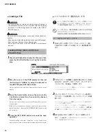
Page 83: ...to save the file to the root directory and root is not shown as Current Dir at the right top of the display press the EXIT button a few times to go to the root directory 5 Press the SF1 EXEC button to execute the Save operation If you are about to overwrite an existing file the display prompts you for confirmation Press the INC YES button to execute the Save operation or press the DEC NO button to...

Page 84: ...irectory select box then select the desired file to be loaded You can select any of the files listed in the Directory File select box on the display If the file is saved under any directory select the directory includ ing the desired file then press the ENTER STORE button to find the desired file 4 Press the SF1 EXEC button to execute the Load operation When the loading is finished Completed will ...

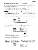
Page 85: ...rogram モードごとに初期化をするかどうか選択をして ファクトリーセットを実行できます 全てのモードを初期化する場合は テストプログラム のファクトリーセットと同様となります Checkbox If you enter a checkmark for a mode name in the display in step 3 below executing the Factory Set will reset the User Memory data or settings of the corresponding mode to the initial factory settings For those modes without checkmarks the User Memory data or settings will be maintained even if Factor...

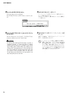
Page 86: ...hile data is being written to Flash ROM never attempt to turn off the power Turning the power off in this state results in loss of all user data and may cause the system to freeze due to corruption of data in the Flash ROM This means that this instrument may not be able to start up properly even when turning the power on next time 4 ENTER STORE ボタンを押します ファクトリーセットを実行してもよいか 確認を求めるメッ セージが画面に表示されます 実行...

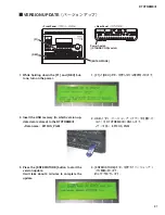
Page 87: ...turn on the power 2 Insert the USB memory to which version up date data is stored to the DTXTREMEⅢ Data name 8F13OS_PGM 3 Press the ENTER STORE button to start the version update It will take about 4 minutes to complete the update 1 F1 と REC ボタンを押しながら電源を入れます 2 USB メモリ バージョンアップデータを置いた もの を DTXTREMEⅢに挿入します データ名 8F13OS PGM 3 ENTER STORE ボタンを押すとバージョンアッ プが開始されます 約 4 分で完了します ...

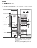
Page 88: ...R B 001 127 USR H 001 127 Drum Kit Edit Click settings Trigger Setup Utility settings Chain Edit Song Record Sampling External USB storage device This diagram details the relationship among the functions of the DTXTREME III and the internal memory and USB storage device File extensions T3C File extensions T3T File extensions T3U File extensions T3H External Drum Kits stored in the root directory o...

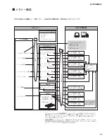
Page 89: ...99 EXT P 01 99 ロード セーブ ストア ユーザーボイス USR A 001 127 USR B 001 127 USR H 001 127 ドラムキットエディット クリック設定 トリガー設定 ユーティリティー設定 チェーンエディット ソング録音 サンプリング 外部USB記憶装置 DTXTREMEⅢ各機能と 内部メモリー USB外部記憶装置との関係は以下のとおりです ファイルタイプ Click ファイルタイプ AllTrigger ファイルタイプ Utility ファイルタイプ AllChain ファイルタイプ AllSong ファイルタイプ AllVoice ファイルタイプ Aiff ファイルタイプ Wav エクスターナルキットはUSB記憶装置のルートディレクトリーに保存 ストア するものですが 本体内部メモリーにロードすることなく 直接選び出して演奏できるキットです エクス...

Page 90: ...alid Try entering a different name Illegal input An invalid input or value has been specified Check the input method or value Illegal sample data The sample file specified for loading is unusable by the DTXTREMEⅢ Illegal selection An unacceptable file has been specified in the Song job mode Illegal song number An unacceptable song number has been specified in the Song job mode Select the song agai...

Page 91: ...Seq data is not empty This message appears if you attempt to record to a track that already contains data Clear the track data in the Song Job mode or select a different track then perform the Record operation Seq memory full The internal memory for Sequence data is full preventing any further operation such as recording Job execution or loading from the USB storage device Try again after erasing ...

Page 92: ...い場合に表示されます Illegal file ロードのとき 目的のファイルが DTXTREMEⅢでは扱えない または現在のモードではロードで きない場合に表示されます Illegal file name ファイルネームが無効の場合表示されます Illegal input 不当な操作や入力を行なったときに表示されます 入力方法や入力値を再度確認してください Illegal sample data DTXTREMEⅢがサポートしていないサンプルファイルを扱おうとした場合に表示されます Illegal selection ファイルモードで選択された内容で実行することができません Illegal song number ソングジョブモードにおいて 指定したソングが不適当な場合に表示されます ソングを選びなお してください Illegal track number ソングジョブモードにおいて 指定...

Page 93: ...メモリーが一杯で サンプリングやジョブ ロードなどが実行できない場合に表示 されます Seq data is not empty シーケンスデータが空でないトラックにレコーディングをしようとした時に表示されます データ をクリアするか 別のトラックを選び もう1度実行してください Seq memory full シーケンサー用の内部メモリーが一杯で レコーディングやジョブの実行 USB記憶装置からの データのロードができないときに表示されます 不要なユーザーソングを消去してから 操作を やりなおしてください System memory crashed フラッシュ ROMへのデータ書き込みに失敗した場合に表示されます Too many stk alt スタック オルタネート用のメモリーがいっぱいで 新規ステップの追加やキットコピーができな い時に表示されます 不要なスタック オルタネート情報...

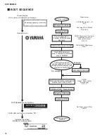
Page 94: ...ied to parameter area of SDRAM Checking for parameter damage judgment is based on damage presence absence judg ment data in flash ROM Damaged Not damaged Executing Factory Set Executing initialization of each device USB Function MIDI SWP51 Initializing SWP51 Tone generator Initializing USB Host Initializing LCDC Startup sequence finished Signal output CPU RESET signal L H IC6 4 Checking CS of SDRA...

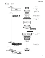
Page 95: ...破壊無し DTXTREMEⅢバナー表示 DAC Mute解除 PTJ5 CN6 27 7SEG LEDの点灯 P01 TOP画面表示 表示される画面は DRUM KIT mode 画面表示無し 立ち上がり シーケンス終了 LCDC初期化 USB Host 初期化 SWP51 音源 初期化 各デバイス初期化実行 USB Function MIDI SWP51 パラメータ破壊判断 Flash ROM上の破壊有無 判断データにより判断 Factory Set 実行 Flash ROMパラメータ 領域をSDRAM上の パラメータ領域へコピー 通常モードProgram実行 boot 部以外の ProgramのSDRAM へのコピー実行 CPU初期化 CPU RESET解除 電源ON SWP51 Reset Reset 解除 2回目 IC25 111 ...

Page 96: ...N OFF Mes All Notes OFF sages Active Sense Reset Notes Mode Default Changed Note ON Note OFF Key s Ch s 0 121 1 16 9nH v 1 127 9nH v 0 9nH v 1 127 9nH v 0 0 127 1 3 1 if MIDI clock out is on 2 if MIDI Sync is midi 3 if Seq Control in out is enabled 0 127 Mode 1 OMNI ON POLY Mode 2 OMNI ON MONO Mode 3 OMNI OFF POLY Mode 4 OMNI OFF MONO 1 16 2 3 0 127 Yes No Default Messages Altered YAMAHA Drum Trig...

Page 97: ...75 91 93 96 97 100 101 0 119 1 95 1 16 1 16 9nH v 1 127 9nH v 0 3 3 4 0 127 1 receive if switch is on 2 m is always treated as 1 regardless of its value 3 depend on HH Ctrl MIDI Type setting 4 depend on Kit Other MIDI CC setting 3 0 127 Mode 1 OMNI ON POLY Mode 2 OMNI ON MONO Mode 3 OMNI OFF POLY Mode 4 OMNI OFF MONO 3 1 16 1 16 v 1 127 1 1 1 1 1 1 1 1 1 120 126 127 121 123 125 1 1 4 m 1 2 0 127 0...

Page 98: ...number as the program number will be selected It is possible to select a drum voice for any MIDI channel except 10 In this case the drum map used for that voice is identical to that for MIDI channel 10 2 2 2 Modulation 1 Reception only 2 2 3 Foot controller 4 Supports both transmission and reception 2 2 4 Portamento time 5 Reception only 2 2 5 Data entry 6 Reception only Used to specify RPN data 2...

Page 99: ...el Aftertouch messages 2 7 Polyphonic Aftertouch Cannot be transmitted and received 3 System Exclusive Messages The DTXTREME III does not receive system exclusive messages that does not include the device number specified with the Device No parameter in the Utility mode 3 1 Universal non realtime messages 3 1 1 GM system ON F0 7E 7F 09 01 F7 Sets all the data except the MIDI master tuning data to i...

Page 100: ...T NO が の部品は サービス用部品として準備されておりません REMARKS 欄の マークの部品は 併用部品です 網掛けの付いた PART NO の 2 番目の文字は ゼロ ではなく オー です 網掛けの付いた PART NO の 2 番目の文字は イチ ではなく アイ です Notes DESTINATION ABBREVIATIONS A Australian model B British model C Canadian model D German model E European model F French model H North European model I Indonesian model J Japanese model K Korean model M South African model O Chinese model Q South east Asi...

Page 101: ...400 250 540 190 410 320 430 410 360 390 380 380 390 280 360 270 580 410 620 30 10 20 20 350 100 480 580 580 530 110 130 560 410 610 600 410 470 410 410 340 50 60 90 60 60 90 60 40 60 Display assembly See page 4 ディスプレイAss y Q P O K A N O F M E L D K C G M L N H I J B G F I J H E D C A B AC adaptor ACアダプター PA 300B PA 300 This figure shows Japanese model この図は 日本モデルです ...

Page 102: ...0 Bonding Screw 3 0X6 MFZN2B3 小 ネ ジ B O N D 3 370 WE774000 Bind Head Screw 3 0X6 MFZN2W3 小 ネ ジ B I N D 2 01 380 WE878000 Bonding Tapping Screw B 3 0X10 MFZN2B3 B タ イ ト B O N D 6 390 WE972200 Bind Head Tapping Screw B 3 0X10 MFZN2B3 B タ イ ト B I N D 9 400 WE975300 PW Head Tapping Screw B 3 0X8 MFZN2B3 B タ イ ト P W H 10 410 WE774300 Bind Head Tapping Screw B 3 0X8 MFZN2W3 B タ イ ト B I N D 41 01 420 Con...

Page 103: ...3 ち ょ う ボ ル ト 4 Label 商 品 ラ ベ ル WC19230 LCD Label L C D ラ ベ ル V218020 GOST R Mark Label G O S T R マ ー ク E WN00110 Russian Leaflet DMI ロ シ ア 注 意 書 D M I E WN67180 Russian Leaflet E ロ シ ア 規 格 詳 細 書 E E WN85560 DTXTREMEⅢ 1 1a 1b Holder Kit ホルダーキット REF NO PART NO DESCRIPTION 部 品 名 REMARKS QTY RANK New Parts RANK Japan only ...

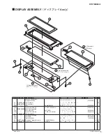
Page 104: ...ト WA54600 30b Connector Assembly LCD BL 2P 220mm L C D B L 束 線 WK46110 40 V8464500 LCD Escutcheon LM L C D エ ス カ ッ シ ョ ン 05 50 LCD Angle Assembly LCDアングルAss y WF21150 50a LCD Angle L C D ア ン グ ル WF16200 50b Insulation Sheet 絶 縁 シ ー ト V320320 2 60 WE774300 Bind Head Tapping Screw B 3 0X8 MFZN2W3 B タ イ ト B I N D 4 01 70 CB829850 Cord Binder S 34B E 束 線 止 め 03 20b 30a 30b 50b 50a 50b 20a 10 60 60 70 ...

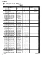
Page 105: ...K RECT チ ッ プ セ ラ B 01 C69 US062470 Ceramic Capacitor SL chip 470P 50V J RECT チ ッ プ セ ラ S L 01 C70 US064100 Ceramic Capacitor B chip 0 0100 50V K RECT チ ッ プ セ ラ B 01 C71 US062470 Ceramic Capacitor SL chip 470P 50V J RECT チ ッ プ セ ラ S L 01 C72 US062470 Ceramic Capacitor SL chip 470P 50V J RECT チ ッ プ セ ラ S L 01 C73 US064100 Ceramic Capacitor B chip 0 0100 50V K RECT チ ッ プ セ ラ B 01 C74 US062470 Ceramic...

Page 106: ...S064100 Ceramic Capacitor B chip 0 0100 50V K RECT チ ッ プ セ ラ B 01 C145 US062470 Ceramic Capacitor SL chip 470P 50V J RECT チ ッ プ セ ラ S L 01 C146 US062470 Ceramic Capacitor SL chip 470P 50V J RECT チ ッ プ セ ラ S L 01 C147 US064100 Ceramic Capacitor B chip 0 0100 50V K RECT チ ッ プ セ ラ B 01 C148 WN561600 Electrolytic Cap chip 10 16V RVL 16V100M チ ッ プ ケ ミ コ ン C151 US064100 Ceramic Capacitor B chip 0 0100 5...

Page 107: ...6 US064100 Ceramic Capacitor B chip 0 0100 50V K RECT チ ッ プ セ ラ B 01 C297 WD758100 Electrolytic Cap chip 22U 6 3V K RECT チ ッ プ ケ ミ コ ン 01 302 WD758100 Electrolytic Cap chip 22U 6 3V K RECT チ ッ プ ケ ミ コ ン 01 C304 US145100 Ceramic Capacitor F chip 0 1000 25V Z RECT チ ッ プ セ ラ F 01 C305 US063100 Ceramic Capacitor B chip 1000P 50V K RECT チ ッ プ セ ラ B 01 C310 US145100 Ceramic Capacitor F chip 0 1000 25V Z...

Page 108: ...ッ プ 抵 抗 01 R73 RD350000 Carbon Resistor chip 0 63M J RECT チ ッ プ 抵 抗 01 R82 RD350000 Carbon Resistor chip 0 63M J RECT チ ッ プ 抵 抗 01 R83 RD350000 Carbon Resistor chip 0 63M J RECT チ ッ プ 抵 抗 01 R90 RD350000 Carbon Resistor chip 0 63M J RECT チ ッ プ 抵 抗 01 R91 RD350000 Carbon Resistor chip 0 63M J RECT チ ッ プ 抵 抗 01 R95 RD354330 Carbon Resistor chip 33 0 63M J RECT チ ッ プ 抵 抗 01 97 RD354330 Carbon Resisto...

Page 109: ...R220 RD357220 Carbon Resistor chip 22 0K 63M J RECT チ ッ プ 抵 抗 01 R221 RD357220 Carbon Resistor chip 22 0K 63M J RECT チ ッ プ 抵 抗 01 R222 RD354470 Carbon Resistor chip 47 0 63M J RECT チ ッ プ 抵 抗 01 R223 RD354470 Carbon Resistor chip 47 0 63M J RECT チ ッ プ 抵 抗 01 R224 RD354680 Carbon Resistor chip 68 0 63M J RECT チ ッ プ 抵 抗 01 R225 RD354470 Carbon Resistor chip 47 0 63M J RECT チ ッ プ 抵 抗 01 R226 RD354470 ...

Page 110: ...0K 63M J RECT チ ッ プ 抵 抗 01 R317 RD356150 Carbon Resistor chip 1 5K 63M J RECT チ ッ プ 抵 抗 01 R318 RD357100 Carbon Resistor chip 10 0K 63M J RECT チ ッ プ 抵 抗 01 R319 RD154270 Carbon Resistor chip 27 0 1 4 J TP チ ッ プ 抵 抗 01 R320 RD154270 Carbon Resistor chip 27 0 1 4 J TP チ ッ プ 抵 抗 01 R321 RD358100 Carbon Resistor chip 100 0K 63M J RECT チ ッ プ 抵 抗 01 R329 RD154270 Carbon Resistor chip 27 0 1 4 J TP チ ッ プ...

Page 111: ...ッ プ 抵 抗 ア レ イ 19 WG890300 Chip Resistor Array 1608X4 33 J チ ッ プ 抵 抗 ア レ イ RA20 WG897100 Chip Resistor Array 1608X4 22K J チ ッ プ 抵 抗 ア レ イ 24 WG897100 Chip Resistor Array 1608X4 22K J チ ッ プ 抵 抗 ア レ イ RA25 WG896300 Chip Resistor Array 1608X4 10K J チ ッ プ 抵 抗 ア レ イ RA26 WG890700 Chip Resistor Array 1608X4 47 J チ ッ プ 抵 抗 ア レ イ 01 RA27 WG890300 Chip Resistor Array 1608X4 33 J チ ッ プ 抵 抗 ア レ イ 29 WG890300 ...

Page 112: ...p chip 0 33 50V RVL 50VR3 チ ッ プ ケ ミ コ ン C131 WC370000 Electrolytic Cap chip 220 00 35 0V チ ッ プ ケ ミ コ ン U D 01 C132 US145100 Ceramic Capacitor F chip 0 1000 25V Z RECT チ ッ プ セ ラ F 01 C133 US145100 Ceramic Capacitor F chip 0 1000 25V Z RECT チ ッ プ セ ラ F 01 C135 US065100 Ceramic Capacitor F chip 0 100 50V Z RECT チ ッ プ セ ラ F 01 C136 US145100 Ceramic Capacitor F chip 0 1000 25V Z RECT チ ッ プ セ ラ F 01 C13...

Page 113: ...EVICE 02 CN107 V6272500 Receptacle Connector 8801 100 170S TE コネクターレセプタクル 05 CN108 WA903400 Connector FMN FMN 34P SE F M N コ ネ ク タ ー CN109 WA903400 Connector FMN FMN 34P SE F M N コ ネ ク タ ー CN110 VB858700 Base Post Connector PH 8P SE ベ ー ス ポ ス ト 01 CN111 WM883300 Connector FFC 52852SHIRI ZU 30P F F C コ ネ ク タ ー CN112 VB858300 Base Post Connector PH 4P SE ベ ー ス ポ ス ト 01 CN113 VB858400 Base Post Conne...

Page 114: ... RD356680 Carbon Resistor chip 6 8K 63M J RECT チ ッ プ 抵 抗 R103 RD257150 Carbon Resistor chip 15 0K 0 1 J RECT チ ッ プ 抵 抗 01 R104 RD356470 Carbon Resistor chip 4 7K 63M J RECT チ ッ プ 抵 抗 01 R105 RF356100 Carbon Resistor chip 1 0K D 1608 チ ッ プ 抵 抗 01 R106 RD154390 Carbon Resistor chip 39 0 1 4 J TP チ ッ プ 抵 抗 R107 RD154390 Carbon Resistor chip 39 0 1 4 J TP チ ッ プ 抵 抗 R108 WA849800 Carbon Resistor chip 8...

Page 115: ...J RECT チ ッ プ 抵 抗 01 324 RD256120 Carbon Resistor chip 1 2K 0 1 J RECT チ ッ プ 抵 抗 01 R325 RF356560 Carbon Resistor chip 5 6K D 1608 チ ッ プ 抵 抗 SW101 V4577800 Push Switch SDKLA10200 プ ッ シ ュ S W STANDBY ON 03 TH1 VV457800 Protector Switch RUEF135 1 35A 30V ポ リ ス イ ッ チ 02 TR102 V4767500 Transistor 2SD0601ARL AQL Q R ト ラ ン ジ ス タ 01 TR103 WC529500 Transistor 2SCKTA1504S Y GR R ト ラ ン ジ ス タ TR104 VD303700 T...

Page 116: ...0 Ceramic Capacitor F chip 0 1000 25V Z RECT チ ッ プ セ ラ F 01 C460 US145100 Ceramic Capacitor F chip 0 1000 25V Z RECT チ ッ プ セ ラ F 01 C462 US145100 Ceramic Capacitor F chip 0 1000 25V Z RECT チ ッ プ セ ラ F 01 C463 UF147470 Electrolytic Cap chip 47 25V チ ッ プ ケ ミ コ ン 01 C465 UF037470 Electrolytic Cap chip 47 16V チ ッ プ ケ ミ コ ン 01 C466 UF147470 Electrolytic Cap chip 47 25V チ ッ プ ケ ミ コ ン 01 C467 US145100 Ce...

Page 117: ...r input 01 JK306 VE382300 Phone Jack YKB21 5010 ホ ー ン コ ネ ク タ RIDE Trigger input 01 JK307 VE382300 Phone Jack YKB21 5010 ホ ー ン コ ネ ク タ CRASH1 Trigger input 01 JK308 VE382300 Phone Jack YKB21 5010 ホ ー ン コ ネ ク タ CRASH2 Trigger input 01 JK309 VE382300 Phone Jack YKB21 5010 ホ ー ン コ ネ ク タ HI HAT Trigger input 01 JK310 VE382300 Phone Jack YKB21 5010 ホ ー ン コ ネ ク タ KICK Trigger input 01 JK311 VE382300 Pho...

Page 118: ...383 RD358100 Carbon Resistor chip 100 0K 63M J RECT チ ッ プ 抵 抗 01 R384 RD357100 Carbon Resistor chip 10 0K 63M J RECT チ ッ プ 抵 抗 01 R385 RD357100 Carbon Resistor chip 10 0K 63M J RECT チ ッ プ 抵 抗 01 R386 RD358100 Carbon Resistor chip 100 0K 63M J RECT チ ッ プ 抵 抗 01 R387 RD358100 Carbon Resistor chip 100 0K 63M J RECT チ ッ プ 抵 抗 01 389 RD358100 Carbon Resistor chip 100 0K 63M J RECT チ ッ プ 抵 抗 01 R390 RF4...

Page 119: ... 01 R470 RD355100 Carbon Resistor chip 100 0 63M J RECT チ ッ プ 抵 抗 01 R471 RD357100 Carbon Resistor chip 10 0K 63M J RECT チ ッ プ 抵 抗 01 478 RD357100 Carbon Resistor chip 10 0K 63M J RECT チ ッ プ 抵 抗 01 R479 RD358100 Carbon Resistor chip 100 0K 63M J RECT チ ッ プ 抵 抗 01 R481 RD358220 Carbon Resistor chip 220 0K 63M J RECT チ ッ プ 抵 抗 01 485 RD358220 Carbon Resistor chip 220 0K 63M J RECT チ ッ プ 抵 抗 01 R486 ...

Page 120: ... Carbon Resistor chip 27 0K D RECT チ ッ プ 抵 抗 R624 RD356100 Carbon Resistor chip 1 0K 63M J RECT チ ッ プ 抵 抗 01 R625 RF457270 Carbon Resistor chip 27 0K D RECT チ ッ プ 抵 抗 R626 RD356100 Carbon Resistor chip 1 0K 63M J RECT チ ッ プ 抵 抗 01 R627 RD356100 Carbon Resistor chip 1 0K 63M J RECT チ ッ プ 抵 抗 01 R628 RF457270 Carbon Resistor chip 27 0K D RECT チ ッ プ 抵 抗 R629 RF457270 Carbon Resistor chip 27 0K D RECT...

Page 121: ... P U R E 01 797 WC895000 Electrolytic Cap PURE 10 0 50 0V RVO ケ ミ コ ン P U R E 01 C802 US145100 Ceramic Capacitor F chip 0 1000 25V Z RECT チ ッ プ セ ラ F 01 C803 US145100 Ceramic Capacitor F chip 0 1000 25V Z RECT チ ッ プ セ ラ F 01 C804 US062100 Ceramic Capacitor SL chip 100P 50V J RECT チ ッ プ セ ラ S L 01 C805 US062100 Ceramic Capacitor SL chip 100P 50V J RECT チ ッ プ セ ラ S L 01 C806 WC895100 Electrolytic Ca...

Page 122: ...XW029A00 IC AK4393VF E2 I C DAC 07 IC707 XW029A00 IC AK4393VF E2 I C DAC 07 IC708 X3505A00 IC NJM2068M D TE2 I C OP AMP 02 IC709 X3505A00 IC NJM2068M D TE2 I C OP AMP 02 IC710 XS537B00 IC NJM2114M TE1 I C OP AMP IC711 XT744B00 IC TC74VHCT245AFT I C TRANSCEIVER 02 IC713 X6789A00 IC DS90LV012ATMF NOPB I C LVDS RECEIVER 05 IC714 X3505A00 IC NJM2068M D TE2 I C OP AMP 02 IC715 X3505A00 IC NJM2068M D TE...

Page 123: ...51 RF356120 Carbon Resistor chip 1 2K D 1608 チ ッ プ 抵 抗 01 758 RF356120 Carbon Resistor chip 1 2K D 1608 チ ッ プ 抵 抗 01 R759 RF356390 Carbon Resistor chip 3 9K D 1608 チ ッ プ 抵 抗 01 762 RF356390 Carbon Resistor chip 3 9K D 1608 チ ッ プ 抵 抗 01 R763 RF356100 Carbon Resistor chip 1 0K D 1608 チ ッ プ 抵 抗 01 770 RF356100 Carbon Resistor chip 1 0K D 1608 チ ッ プ 抵 抗 01 R771 RF356390 Carbon Resistor chip 3 9K D 160...

Page 124: ...5 0 1W J 酸 化 金 属 被 膜 抵 抗 01 R876 RD156100 Carbon Resistor chip 1 0K 1 4 J TP チ ッ プ 抵 抗 R877 RD256120 Carbon Resistor chip 1 2K 0 1 J RECT チ ッ プ 抵 抗 01 R878 RD256120 Carbon Resistor chip 1 2K 0 1 J RECT チ ッ プ 抵 抗 01 RA702 WH211800 Resistor Array 10K X 4 抵 抗 ア レ イ 704 WH211800 Resistor Array 10K X 4 抵 抗 ア レ イ RA705 WH206600 Resistor Array 68 X 4 抵 抗 ア レ イ 01 RA706 WH206600 Resistor Array 68 X 4 抵 抗 ...

Page 125: ...ide Volume B10K RS30111A9 30mm ス ラ イ ド V R 3 0 M M CLICK 03 VR702 VH335400 Slide Volume B10K RS30111A9 30mm ス ラ イ ド V R 3 0 M M ACCOMP 03 VR703 VH335400 Slide Volume B10K RS30111A9 30mm ス ラ イ ド V R 3 0 M M KICK 03 VR704 VH335400 Slide Volume B10K RS30111A9 30mm ス ラ イ ド V R 3 0 M M SNARE 03 VR705 VH335400 Slide Volume B10K RS30111A9 30mm ス ラ イ ド V R 3 0 M M TOM 03 VR706 VH335400 Slide Volume B10K R...

Page 126: ...GULATOR 12V REGULATOR 5V DC DC CONVERTER 6 5V IC112 3P IC101 3P IC124 5P REGULATOR 9V DAC CPU SWP51 SDRAM IC26 54P SDRAM FLASH ROM FLASH ROM IC36 IC37 48P IC39 IC40 48P CN19 168P CN20 168P WAVE ROM L 128M WAVE ROM H 128M SDRAM INDIVIDUAL OUTPUT USB MIDI OUTPUT CN702 34P CN707 3P CN303 3P CN301 15P CN13 15P CN706 4P CN112 4P CN108 34P LCD display Back light SW701 SW735 LD701 LD712 VR703 VR708 VR701...

Page 127: ...K46090 Connector Assembly DM CN12 WM501700 SUB DM DM CN18 WK46100 MPX MIC DM CN11 WK46110 MIDI DM CN7 DIMM Socket DMSUB CN112 168P WK76990 E BUS JK CN303 168P WM501300 SUB PN DMSUB CN109 WM501500 PN JK SW LCD WK46060 FFC Cable Back Light LED WK46080 DM CN5 DM CN19 LCD DM CN20 LCD BL Receptacle Connector DIMM Socket No Unit Name ユニット名 Location No ロケーション番号 Part No 部品番号 Remarks 備考 460 470 480 450 440...

Page 128: ...R 1 9V SYSTEM RESET 2 9V OR AND BUS BUFFER INVERTER TRANSCEIVER TRANSCEIVER TRANSCEIVER TRANSCEIVER TRANSCEIVER TRANSCEIVER SWP51 SDRAM 64M EFFECT BUFFER TRANSCEIVER CPU FLASH ROM SUB FLASH ROM MAIN SDRAM 64M SDRAM 64M USB POWER SWITCH OR Photo Coupler INVERTER to DMSUB CN107 Page 5 F 5 to DMSUB CN113 Page 5 G 4 to PN CN704 Page 5 J 4 to DMSUB CN110 Page 5 H 3 to DMSUB CN104 Page 5 H 2 to DMSUB CN...

Page 129: ...UIT DIAGRAM 2 4 DM 2 2 Page 4 DTXTREME DTXTREME DTXTREME 28CC1 2001033266 2 REGULATOR 1 5V WAVE ROM L 128M WAVE ROM L 128M WAVE ROM H 128M SWP51 WAVE ROM H 128M Not installed Not installed Not installed Not installed not installed 未実装部品 to DMSUB CN101 Page 5 G 2 D1F60 VS201100 DIODE 1A 600V DM D3 1 ANODE 2 CATHODE 2 1 LMS8117AMP ADJ X0609A00 REGULATOR 1 9V DM IC35 1 ADJ GND 2 OUTPUT 3 INPUT 1 2 3 ...

Page 130: ... 1 2 3 4 7 8 6 5 NJM79M12DL1A X2593A00 REGULATOR 12V DMSUB IC120 1 COMMON 2 INPUT 3 OUTPUT 1 2 3 PQ1CY1032ZPH X5090A00 DC DC CONVERTER DMSUB IC102 108 124 1 V IN 2 V OUT 3 COM heat sink 4 O adj 5 V soft 1 5 PQ200WNA1ZPH X7964A00 REGULATOR 12V DMSUB IC123 1 DC INPUT 2 ON OFF CONTROL 3 DC OUTPUT 4 VOLTAGE ADJUST 5 GND 1 2 3 4 5 BA50BCOFP E2 X8260A00 REGULATOR 5V DMSUB IC101 1 2 3 1 INPUT 2 GND 3 OUT...

Page 131: ...MP OP AMP OP AMP OP AMP OP AMP OP AMP OP AMP OP AMP OP AMP OP AMP OP AMP OP AMP OP AMP OP AMP OP AMP OP AMP OP AMP OP AMP OP AMP OP AMP OP AMP OP AMP OP AMP OP AMP OP AMP OP AMP OP AMP OP AMP MULTIPLEXER TRANSCEIVER TRANSCEIVER TRANSCEIVER OR OR OR OR TRANSCEIVER TRANSCEIVER MULTIPLEXER OP AMP OP AMP REGULATOR 5V to DM CN13 Page 3 L 1 to PN CN707 Page 5 L 10 to DMSUB CN109 Page 5 I 4 RB500V 40 V23...

Reviews: