background image

DVD-S559

28

2

1

3

4

5

6

7

8

2

1

3

4

5

6

7

8

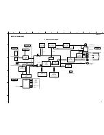
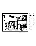
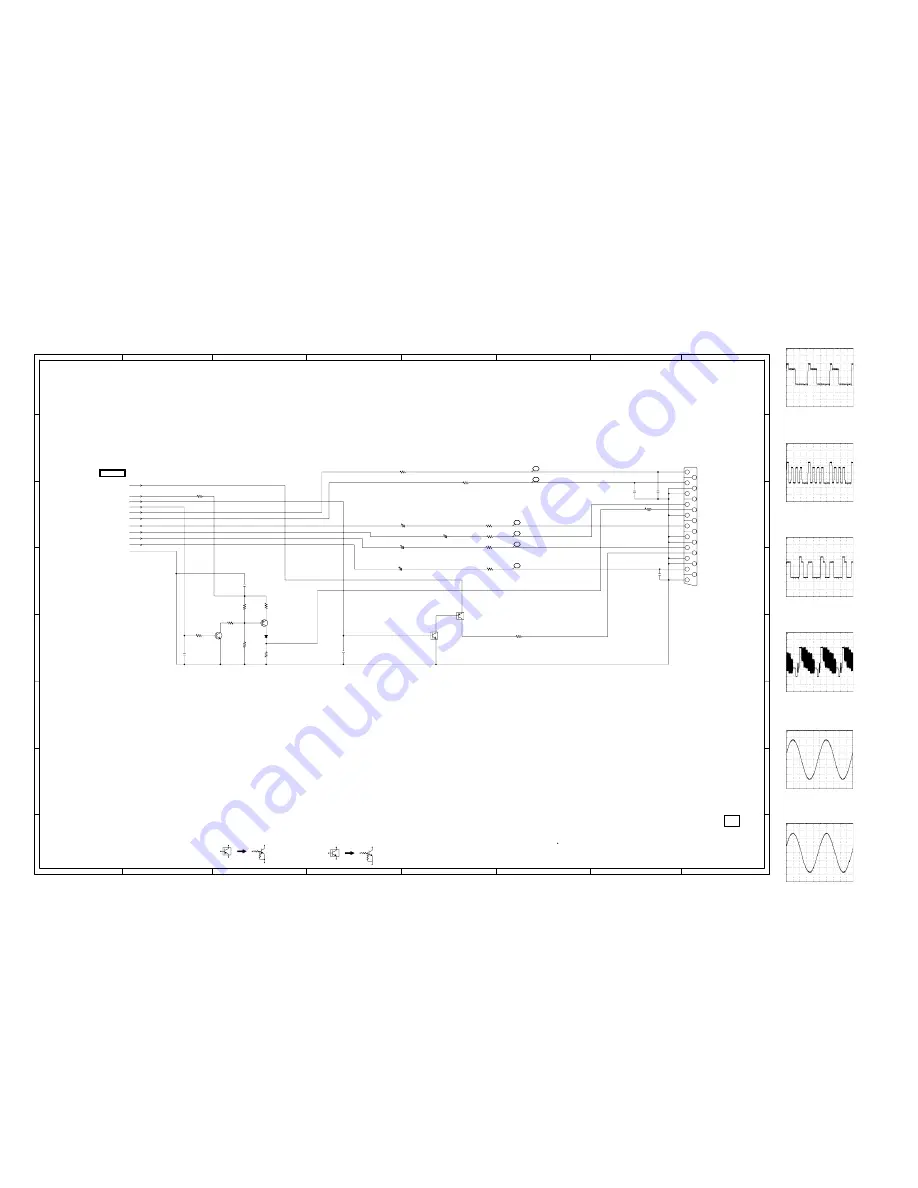
CAUTION: DIGITAL TRANSISTOR

Q8105

DTA114EKA

DVD_RGB_H_OUT

J8101

MRC-021V-07_A

21PIN CONNECTOR

1

10

11

12

13

14

15

16

17

18

19

2

20

21

3

4

5

6

7

8

9

L8101

10uH 0305

Q8104

DTC144EKA

DVD_RGB_H_OUT

D8101

1SS355

CAUTION: DIGITAL TRANSISTOR

Q8101

KTC3875S_Y_RTK

21PIN CTL IN

Q8102

KTA1504S_Y_RTK

21PIN CTL DRV

R8115

220 +-1%

R8114

220 +-1%

R8109

68 +-1%

R8110

75 +-1%

R8112

75 +-1%

R8113

75 +-1%

R8111

75 +-1%

R8120

1 1/4W

R8101

4.7K 1/4W

R8105

390 1/4W

R8104

6.8K

R8108

8.2K

R8103

470

1/4W

R8102

56K

C8107

0.001

B

C8111

0.001

B

C8116

33P

CH

C8106

0.001

B

C8101

0.01

B

C8105

0.1

B

C8113

470

6.3V

YK

C8115

1000

6.3V

YK

C8114

470

6.3V

YK

C8112

1000

6.3V

YK

DURING PLAYBACK.

MEASURED WITH THE DIGITAL TESTER

NOTE:THE DC VOLTAGE EACH PART WAS

OF PRINTING AND SUBJECT TO CHANGE WITHOUT NOTICE

NOTE: THIS SCHEMATIC DIAGRAM IS THE LATEST AT THE TIME

21PIN_R

21PIN_L

AT+3.3V

P.CON+12V

P-H/I-L_RGB-H

ASP/FS

21PIN_CTL

AMP_A_OUT_R

AMP_A_OUT_L

DAC_A[G]Y_VIDEO

21PIN/D_G/Y_OUT

DAC_C[B]U_VIDEO

21PIN/D_B/U_OUT

DAC_B[R]V_VIDEO

21PIN_CVBS_VIDEO

21PIN/D_R/V_OUT

A_GND

BLANKING_OUT

21PIN_CVBS_OUT

NC

NC

NC

NC

NC

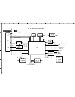
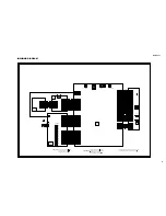
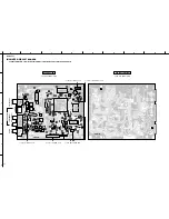
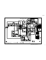
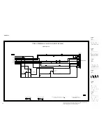
21PIN/D-TERMINAL/DIGITAL AUDIO SCHEMATIC DIAGRAM

(POWER PCB 2/2)

0

3.2

3.3

0

0

3.2

21

22

23

25

26

24

FROM POWER

12.1

11.4

11.4

12.1

0

0

PCB240
DPE004

A

B

C

D

E

F

G

H

A

B

C

D

E

F

G

H

AV (SCART)

Point 

a

20 

µ

s

500 mV

Point 

s

20 

µ

s

500 mV

Point 

d

20 

µ

s

500 mV

Point 

f

20 

µ

s

500 mV

Point 

g

200 

µ

s

1.0 V

Point 

h

200 

µ

s

1.0 V

* Components having special characteristics are marked 

Z

 and must be replaced with

parts having specifications equal to those originally installed.

* Schematic diagram is subject to change without notice.

Summary of Contents for DVD-S559

Page 1: ...ice departments of YAMAHA are continually striving to improve YAMAHA products Modifications are therefore inevitable and specifications are subject to change without notice or obligation to retrofit Should any discrepancy appear to exist please contact the distributor s Service Division WARNING Static discharges can destroy expensive components Discharge any static electricity your body may have a...

Page 2: ... between solder and your skin When soldering do not inhale solder fumes or expose eyes to solder flux vapor If you come in contact with solder or components located inside the enclosure of this product wash your hands before handling food Side A Side B DVD P C B Lead Free Solder Lead Free Solder POWER P C B Lead Free Solder OPERATION 1 P C B Lead Free Solder OPERATION 2 P C B Lead Free Solder Abou...

Page 3: ... laser compo nent will emit a beam for several seconds to detect if a disc is present During this time 5 10 sec the laser may radiate through the lens of the laser pick up unit Do not attempt any servicing during this period If no disc is detected the laser will stop emitting the beam When a disc is loaded you will not be exposed to any laser emissions 2 The laser power level can be adjusted with ...

Page 4: ...actured to respond to the Locale Management Information that is recorded on a DVD disc If the Locale number described on the DVD disc does not correspond to the Locale number of this DVD player this DVD player cannot play this disc 1MΩ Conductive material sheet or steel sheet Anti static wrist strap 1 4 4 2 2 2 3 6 5 5 5 This product incorporates copyright protection technology that is protected b...

Page 5: ...DVD S559 5 DVD S559 FRONT PANEL REAR PANEL WG11920 DVD REMOTE CONTROL ...

Page 6: ...al System DVD player Power requirements AC 220 240 V 50 60 Hz Power consumption 7 W Power consumption standby 0 7 W Weight 1 8 kg 3 lbs 15 oz Dimensions W x H x D 435 mm x 61 mm x 213 mm 17 1 8 x 2 3 8 x 8 3 8 Finish Black color Silver color Accessories Audio video cable x 1 Power cable x 1 Remote control x 1 AA R6 dry cell batteries x 2 Manufactured under license from Dolby Laboratories Dolby and...

Page 7: ...559 7 DVD S559 DIMENSIONS 435 17 1 8 205 8 1 16 6 1 4 13 1 2 2 1 16 48 1 7 8 61 2 3 8 213 8 3 8 INTERNAL VIEW 1 2 3 5 4 1 POWER P C B 2 DVD Mechanism Unit 3 DVD P C B 4 OPERATION 1 P C B 5 OPERATION 2 P C B ...

Page 8: ...soldering conditions Soldering temperature 320 20 C Soldering time Within 3 seconds Soldering combination Sn 3 0Ag 0 5Cu When Soldering Removing of solder use the draw in equipment over the Pick Up Unit to prevent the Flux smoke from it Short circuit using a soldering iron Pick Up P C B DVD Mechanism Unit DVD P C B CP2301 Fig 1 The laser diode used for a pickup head may be destroyed with external ...

Page 9: ...red Disconnect the power cable from the AC outlet How to manually eject the tray Fig 1 a Turn the player bottom up b Move the slider in the direction indicated with a screw driver until the tray is ejected c Gently pull the tray out a b c Frame Rear Front Tray Screw Driver Slider Fig 1 ...

Page 10: ...g successively 4 snaps 2 on the side and 2 on the bottom g Remove the Front Cabinet The Sheet Earth once removed cannot be reused Be sure to use a new Sheet Earth for replacement 3 Removal of OPERATION 1 and OPERATION 2 P C B s Fig 2 a Remove 4 screws 4 b Remove the OPERATION 1 P C B c Remove 1 cable connection CP603 d Remove 3 screws 5 e Remove the OPERATION 2 P C B Fig 2 1 1 1 1 CP4002 Sheet Ear...

Page 11: ...a soldering iron If you remove the DVD Mechanism Unit with no soldering the Laser may be damaged b Remove 4 screws 6 c Remove 3 cable connections CP2301 CP2302 CP2303 d Remove the DVD Mechanism Unit 6 6 6 6 DVD Mechanism Unit CP2301 Short circuit using a soldering iron Pick Up P C B Solder CP2303 CP2302 Fig 3 ...

Page 12: ...2 screws 8 b Remove 3 cable connections CP503 CP4001 CP4003 c Remove the POWER P C B 6 Removal of DVD P C B Fig 5 a Remove 4 screws 9 and 4 screws 0 b Remove the DVD P C B in the direction of arrow B 7 7 7 8 8 7 POWER P C B CP503 CP4003 CP4001 9 9 9 10 9 DVD P C B B Fig 4 Fig 5 ...

Page 13: ... of IC4001 pin 5 SDA and pin 6 SCL on the DVD P C B Ass y fluctuating for one or two seconds after the power is turned Check the video signal path between DVD IC IC4002 on the DVD P C B Ass y and Video out J8001 terminal Does the voltage of CP2302 pin 3 and pin 1 on the DVD P C B Ass y change normally SW 1 pin 3 OPEN on the DVD Mechanism Unit Tray is fully opened L SW 2 pin 5 CLOSE on the DVD Mech...

Page 14: ... deteriorate If the voltage at each both ends of R2302 and R2304 on the DVD Mechanism Unit is 0 4 V or more the 780 nm LD is definitely deteriorated Are there scratches or dirt on the disc Are there scratches or dirt on the disc Is there a problem with the format of the disc Check the waveform IC4002 213pin ALRCK 214pin ABCK 215pin ACLK 217pin ASDATA Is signal output from IC8004 pin 7 and pin 8 on...

Page 15: ...F URST D_AUDIO ZERO AUDIO_L R AUDIO_L R LD IR 108MHz TV ENCODER MPEG 1 2 JPEG VIDEO DECODER AUDIO CODEC R S_VIDEO COAXIAL RF AMP U CO L OVERALL BLOCK DIAGRAM IR RECEIVER OS651 IC4004 16Mbit FLASH S29AL016D70TFI020 IC4005 64Mbit SDRAM K4S641632H UC75 SDA SCL S IC4003 RESET IC BD5229G TR IC8001 VIDEO SW IC SN74CBT3257PWR V Y CV 21 PIN CVBS RGB 23 21 26 225 110 1 7 AUDIO OUT L R AV SCART VIDEO OUT VI...

Page 16: ...IVE LA6565 TE L E DMSO FMSO TROPEN TRCLOSE TRSO FOSO STBY V1P4 T F LOAD MOT_SLED MOT_SPDL OPU SPINDLE STEPPING SLED MOTOR LIMIT TRIN TROUT OPO OP IC4004 16Mbit FLASH S29AL016D70TFI020 A IC4005 64Mbit SDRAM K4S641632H UC75 A MA0 MA11 DQ0 DQ15 DCS DRAS DCAS DWE DBA0 DBA1 SDCLK0 SDCKE DQM0 DQM1 IC8004 AUDIO DAC 2CH PCM1742KE 2K IR VIDEO AUDIO FIP BLOCK FP_DI FP_DO FP_SCK STB FLDC R CR B CB G Y C V 4C...

Page 17: ... S V Y VIDEO JACK J8001 S S JACK J8002 S_Y S_C IC8003 AUDIO AMP IC BA4560F E2 G AUDIO_L R I XP LETTER SQUEEZE VSEL1 VSEL1 SQUEEZE AUDIO_L R VSEL1 I XP LETTER SQUEEZE L MUTE Tr F R AUDIO JACK J8003 ZERO COAXIAL DRIVE D COA ASPDIF COAXIAL J8004 IC651 FIP DRIVER IC PT6315 GR1 GR8 P1 P16 FIP V651 8 BT 234GNK IR IR RECEIVER OS651 A FP_DI FP_DO FP_SCK STB FLDC IR A H Y CB CR OPERATION 1 A B C D E F G H ...

Page 18: ...V SW Q510 P CON 12V SW Q8101 Q8102 Q504 FL P CON SW Q502 28V P CON SW VOLTAGE CTL IC501 KIA431A AT PHOTO COUPLER IC504 PS2561AL1 1 V W POWER CTL IC502 STR A6151M 6V REG IC503 PQ070XF01SZH Q8104 Q8105 DVD_RGB_H_OUT 21 PIN CTL AT 3 3V 21 PIN CTL BLANKING_OUT CP503 CP8001 FFC CONNECTOR ASP FS P H I L _RGB H J8101 21PIN CONNECTOR P CON 12V G_VIDEO B_VIDEO R_VIDEO CVBS_VIDEO AUDIO_R AUDIO_L AV SCART ...

Page 19: ...D B VR780 CD VRF RF_OUT SW1 DVD CD C E VS F GND A VR650 DVD GND GND LD_DVD 650 LD_CD 780 PD GND NC VRCOM TRKG DRV TRKG RTN FOCS RTN FOCS DRV VCC D B VR780 CD VRF RF_OUT SW1 DVD CD C E VS F GND A VR650 DVD GND GND LD_DVD 650 LD_CD 780 PD GND NC TXD RXD V 3D NC NC NC NC NC CP8001 R CR G Y B CB GND GND RGB H FS AUDIO L GND AUDIO R CVBS GND 12 12 11 11 10 9 8 7 6 5 4 3 2 1 10 9 8 7 6 5 4 3 2 1 11 10 9...

Page 20: ...098 C4099 W851 B4001 R4033 C4052 C4093 B4002 C4040 C4081 C2305 C4046 C4103 C4104 C4102 C4101 C2323 R2329 R2319 R2331 R2342 C2322 W819 C4105 R4003 C4091 CP8001 IC8002 IC8004 R8028 R8029 R8024 R8027 R8040 R8039 R8076 R8078 R8056 R8046 R8044 R8083 R8081 R8054 R8077 R8084 R8079 R8074 R8061 R8049 R8059 R8057 R8082 R8085 R8080 R8073 R8066 R8070 R8023 R8026 R8051 Q8013 Q8010 Q8020 Q8019 Q8021 Q8018 B8004...

Page 21: ... Q512 Q503 Q511 Q509 R541 R543 R509 Q505 Q513 R544 R537 R536 R531 C507 C541 C501 R545 R526 R519 R547 R8108 R8102 C8116 C8111 C8107 C8106 C8101 Q8104 R8115 R8114 R8110 R8111 R8112 R8113 R8109 C8105 R8104 Q8102 Q8101 Q8105 D8101 DPE004B DPE004B R IS K O F F IR E R E P L A C E A S M A R K E D AC IN AV SCART To CP4003 of DVD P C B To CP8001 of DVD P C B To PC4001 of DVD P C B POEWR INSERTED PARTS SOLD...

Page 22: ...Q3 MA0 DQ4 MA10 DQ5 V 3 TROUT DBA1 DQ6 TRIN RXD DQ7 DQ8 STBY DBA0 TXD DQ9 TRCLOSE D_GND DQ10 DQ11 DCS A2 DQ12 DRAS DQ13 A3 DCAS DQ14 A4 DWE DQ15 A5 A0 A6 DQM1 A1 A2 A7 DQ8 FP_SCK A3 A8 FP_DI A4 A18 DQ9 A5 STB A19 DQ10 A6 FP_DO A7 DQ11 A8 DQ12 IR SDA A9 DQ13 SCL V 3E A10 A11 V 3 A12 URST A13 UWR URD A14 FLDC A15 28V A16 V 3E A17 FLDC A18 A19 A20 AD0 AD1 AD2 AD3 AD4 AD5 AD6 PWR DQM0 DQ15 DQ14 A16 A1...

Page 23: ... MA11 DBA0 A17 A7 A18 A19 MA9 DBA1 A20 AD0 A6 AD0 AD1 MA8 MA10 AD2 PRD A5 AD3 AD4 MA7 MA0 AD5 A4 AD6 AD7 MA6 MA1 PRD PCE A3 PCE PWR MA5 MA2 A1 A2 MA4 MA3 V 3 D_GND FROM POWER PORT PCB130 DME025 0 0 1 4 2 6 2 6 1 4 1 2 1 6 1 6 3 3 1 3 0 9 1 6 2 5 1 5 1 6 1 3 2 5 1 5 0 8 1 0 1 7 0 0 1 0 0 3 3 1 6 0 8 0 0 7 0 6 1 2 1 3 1 9 0 7 1 2 3 3 A16 VSS VSS A0 A7 A6 A5 A4 A3 A2 A1 A15 A14 A13 A12 A11 A9 A8 A18 ...

Page 24: ...GE WITHOUT NOTICE NOTE THIS SCHEMATIC DIAGRAM IS THE LATEST AT THE TIME IOA V 5S RF DEICG DEICG V 5S V20 A B F C V20 D E V 3F F E MDI1 D LDO2 C LDO1 IOA IOA LDO1 RF V1P4 LIMIT B TROUT A TRIN STBY MDI1 DMSO FMSO TRCLOSE TROPEN PWMOUT1 TRSO LDO2 FOSO OPO OP OP T T F F V 6A V 3F TRSO FOSO V 5S D_GND M_GND LOAD LOAD STBY TROUT V 6A DMSO TRIN V1P4 OPO OP OP LIMIT MOT_SLED MOT_SLED MOT_SPDL MOT_SPDL V 3...

Page 25: ... W824 W866 W870 IC8003 BA4560F E2 AUDIO LPF AMP IC 1 2 3 4 5 6 7 8 DURING PLAYBACK MEASURED WITH THE DIGITAL TESTER NOTE THE DC VOLTAGE EACH PART WAS B8001 MMZ1608R102CT B8003 MMZ1608R102CT B8006 MMZ1608R102CT B8007 MMZ1608R102CT B8004 MMZ1608R102CT B8002 MMZ1608R102CT OF PRINTING AND SUBJECT TO CHANGE WITHOUT NOTICE NOTE THIS SCHEMATIC DIAGRAM IS THE LATEST AT THE TIME SD SCK V 12AT V 5A V 3A ALR...

Page 26: ...WITHOUT NOTICE NOTE THIS SCHEMATIC DIAGRAM IS THE LATEST AT THE TIME V 3A V 5A V 5A V 5V V 5V V 12AT V 12AT V 12 V 12 V 6A D_GND V 5S V 6A V 5S V 3F V 3F D_GND M_GND V 3A V 3 V 3 V 3E V 3E V 1R8 V 1R8 V 3A FLDC POWER_ON FLDC 28V D_GND V 3 D_GND DVD PCB 5 5 POWER PORT SCHEMATIC DIAGRAM TO MEMORY TO LOADER MOTOR DRIVE TO AUDIO VIDEO JACK CP502 FROM TO POWER PCB130 DME025 OPU MOTOR CORE MPEG SDRAM FL...

Page 27: ... 1 5M 1 2W R504 680K R526 6 8K 1 R545 22K 1 R546 3 3K M 1 R524 1K 1 4W R519 1K R525 150 1 4W R530 560 1 4W R528 22K 1 4W R541 5 6K 1 R542 1K 1 R543 4 7K 1 R540 680 1 4W R509 1K R547 22 R537 1K R544 10K R534 100 1 4W R539 4 7K 1 4W R506 100 R538 22K R514 1K 1 4W R513 10K 1 4W R518 3 3K 1 R517 1 2K 1 R516 10 R531 10K R536 10K R505 22 1 4W C502_2 0 22 275V ECQUL C518 0 001 KX C505 100P 2KV R C516 0 0...

Page 28: ...AL TESTER NOTE THE DC VOLTAGE EACH PART WAS OF PRINTING AND SUBJECT TO CHANGE WITHOUT NOTICE NOTE THIS SCHEMATIC DIAGRAM IS THE LATEST AT THE TIME 21PIN_R 21PIN_L AT 3 3V P CON 12V P H I L_RGB H ASP FS 21PIN_CTL AMP_A_OUT_R AMP_A_OUT_L DAC_A G Y_VIDEO 21PIN D_G Y_OUT DAC_C B U_VIDEO 21PIN D_B U_OUT DAC_B R V_VIDEO 21PIN_CVBS_VIDEO 21PIN D_R V_OUT A_GND BLANKING_OUT 21PIN_CVBS_OUT NC NC NC NC NC 21...

Page 29: ...4 GR3 GR2 GR1 28V P8 P9 P10 P11 P12 P13 P14 P15 P16 P7 P6 P5 STB P4 FP_SCK P3 FP_DI P2 FP_DO P1 GR8 GR7 GR6 GR5 GR4 GR3 GR2 GR1 FP_SCK FP_DI STB FP_DO V 3E IR IR V 3E V 3E FLDC 28V FLDC GND OPERATION 1 PCB DISPLAY SCHEMATIC DIAGRAM PCB270 DEE029 NC STB 12 23 12 0 6 0 18 0 3 2 0 0 0 5 1 19 0 15 6 19 0 9 5 13 0 9 5 12 6 6 0 LED1 LED2 LED4 CLK 34 VDD 44 NC NC NC NC 18 0 18 0 18 0 18 0 18 0 18 0 18 0 ...

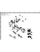
Page 30: ... 112 101 116 116 PCB240 PCB280 PCB270 PCB130 SILVER model The Sheet Earth once removed cannot be reused Be sure to use a new Sheet Earth for replacement SILVER model REPLACEMENT PARTS LIST EXPLODED VIEW Note Those parts without Ref No are not supplied as spare parts ...

Page 31: ...5550 DVD MECHANISM UNIT DM 4 A2G539A650 PCB130 AAX75560 P C B ASS Y DVD A2G540A130 Z PCB240 AAX75600 P C B ASS Y POWER F2G502A24B PCB270 AAX75570 P C B ASS Y OPERATION1 BL A2G539A270 PCB270 AAX75580 P C B ASS Y OPERATION1 SI A2G540A270 PCB280 AAX75590 P C B ASS Y OPERATION2 A2G540A280 ACCESSORIES 1000 WG119200 REMOTE CONTROL RR3899 1301EM 07650LZ010 1000 1 AAX07830 BATTERY COVER 103RRS 093 01R Z 1...

Page 32: ...0 18 17 32 31 30 29 28 27 26 25 40 39 37 36 35 34 33 41 uPD678MC 855 5A4 E1 A D1 MIE 554A2 R1 2ohms R2 27ohms Q1 2SC3440 T112 C1 T1 3 0V 47uF C2 1 2 3 4 5 6 7 8 9 10 20 19 18 17 16 15 SW1 JP1 JP2 JP3 14 13 12 11 K1 06 K1 07 S0 S1 REM VDD OSC OUT OSC IN VSS S2 K1 05 K1 04 K1 03 K1 02 K1 01 K1 00 K13 K12 K11 K10 0 1uF X1 4 00MHz ...

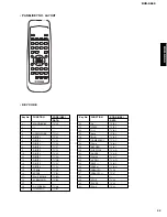
Page 33: ... 8 DIGIT 9 DIGIT 0 CLEAR ENTER PLAY MODE SURROUND ON SCREEN TOP MENU CODE HEX DATA 7C 80 7C 81 7C 94 7C 95 7C 96 7C 97 7C 98 7C 99 7C 9A 7C 9B 7C 9C 7C 93 7C 9F 7C B8 7C BD 7C E3 7C A6 7C B1 Key No 22 23 24 25 26 27 28 29 30 31 32 33 34 35 36 37 38 39 40 41 FUNCTION Up MENU Left Enter Right HOME MENU Down RETURN SUBTITLE ANGLE ZOOM AUDIO SKIP SHIP SERACH SERACH STOP PAUSE PLAY CODE HEX DATA 7C B4 ...

Page 34: ...DVD S559 ...

Reviews: