GX-900
GX-900
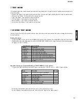
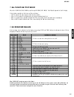
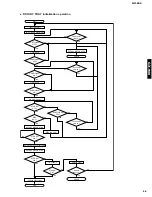
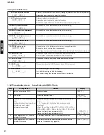
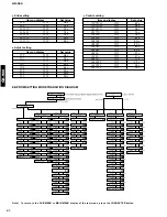
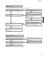
Description of TEST modes
1. AUTO pre-adjustment mode
Automatic pre-adjustment is performed. (Grating adjustment mode after this adjustment.)
[ _
AUT
_
YOBI
_ ]
Adjusted values are output by using the interface.
2. AUTO adjustment mode
Automatic adjustment is performed.
[
AUTO
_
AJST
_ ]
Adjusted values are output by using the interface.
Continuous reproduction is performed. (Error rate on display, jump test)
3. RESULT preparation mode
Not used (Do not use this function as it is not for servicing)
[ _
RST
_
YOBI
_ ]
4. RESULT mode (main adjustment)
Not used (Do not use this function as it is not for servicing)
[ _
RESULT
_ _ _ ]
5. MANUAL pre-adjustment mode
Not used (Do not use this function as it is not for servicing)
[ _
MNU
_
YOBI
_ ]
6. MANUAL adjustment mode
Not used (Do not use this function as it is not for servicing)
[ _
MNU
_
AJST
_ ]
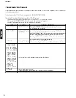
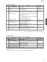
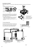
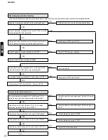
7. EEPROM setting mode
Various factors of the digital servo function are changed manually.
[
EEPROM
_
SET
]
Each servo function is turned on independently.
The voltage is measured at the temperature detect terminal and the standard value is set.
8. TEST-PLAY mode
Continuous reproduction from the specified address is performed.
[
TEST
_
PLAY
_ ]
C1 error rate is measured and ADIP error rate is measured.
9. TEST-REC mode
Continuous recording from the specified address is performed.
[
TEST
_
REC
_ _ ]
10. INNER mode
The position where the INNER switch is turned ON is measured.
[ _ _
INNER
_ _ _ ]
11. EJECT mode
To TEMP setting (of EEPROM setting)
[ _ _
EJECT
_ _ _ ]
To CONTROL setting (of EEPROM setting)
Laser power setting (record/reproduction power) is performed.
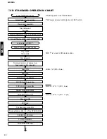
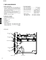
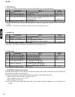
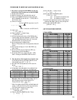
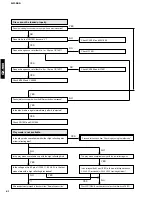
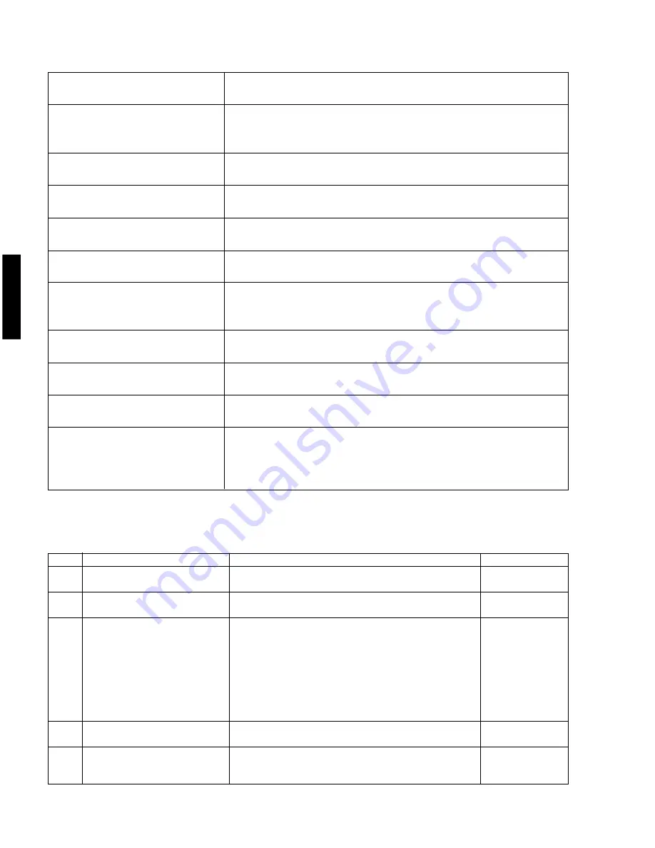
1. AUTO pre-adjustment mode
Low reflecting disc (MMD-318) only
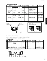
Step
Setting method
Remark
Display
1
2
3
4
5
Set the Test mode to STOP.
Load a disc.
Press the REC/PAUSE(MD) button
once.
Grating adjustment is performed and
adjusted values are output.
Adjustment is completed.
When adjustment is OK, press the
CHARACTER button.
When adjustment is NG, press the
CHARACTER button.
No disc is loaded.
Auto pre-adjustment menu
Auto pre-adjustment is started after sliding to the innermost
track.
“
***
” changes in the following order during automatic
adjustment.
HAo -> RFg -> SAg -> SBg -> PTG -> PCH -> GTG -> GCH ->
RCG -> SEG -> RFG -> SAG -> HAO -> HEO -> TCO -> LAO
Proceed to Step 4 when adjustment is OK.
Proceed to Step 5 when adjustment is NG.
The display returns to the AUTO pre-adjustment menu.
There is an abnormality at the adjusted point such as HAo.
Refer to “Troubleshooting”. (page 40)
[
EJECT
]
[
LOADING
]
[ _
AUT
_
YOBI
_ ]
[
***
: _ _ _ _ _ _ ]
[ _
COMPLETE
_ ]
[
Can't
_
ADJ.
]
[ _
AUT
_
YOBI
_ ]
[
Can't
_
ADJ.
]
31
Summary of Contents for GX-900
Page 103: ...GX 900 GX 900 ...