background image

31

AN200

C-6   MIDI

After connecting the MIDI IN to the MIDI OUT via a MIDI cable,

execute the test. MIDI IN transmits the test pattern (AA 50 5F) to be

received by MIDI IN.

Display of Test Results

OK:


NG:


Test End

The test result is displayed and the test will be finished.

C-7   WAVE ROM

This is the data read/ verify check for the WAVE ROM.

Display of Test Results

OK:


NG:


Test End

The test result is displayed and the test will be finished.

Refer to “The test procedure when an error is detected” when “NG”

(No Good) error is detected.

C-8   1kHz OUTPUT-L

Insert the appropriate phone plugs into each output jack of the OUT-

PUT (L, R) and PHONE (L, R), and then connect them to a fre-

quency counter, oscilloscope and AC volt meter.

The VOLUME control must be set at maximum.

Verify that the following signals are output from OUTPUT-L and

PHONES-L.

OUTPUT-L:

1kHz +/- 3Hz Asine wave,+3.0 +/- 2dBm (load 10k

),Distortion: less than 0.6%

OUTPUT-R:

less than -80dBm(load 10k 

)

PHONES-L:

-4.0 +/- 2 dBm (load 33 

) ADistortion: less than

0.6%

PHONES-R:

less than -60dBm(load 33 

)

Display of Test Results

Not appearing

Test End

Rotate [DATA ENTRY] knob clockwise to proceed to the next test.

C-9   1kHz OUTPUT-R

Insert the appropriate phone plugs into each output jack of the OUT-

PUT (L, R) and PHONE (L, R), and then connect them to a fre-

quency counter, oscilloscope and AC volt meter.

The VOLUME control must be set at maximum.

Verify that the following signals are output from OUTPUT-R and

PHONES-R.

OUTPUT-L:

less than -80dBm(load 10k 

)

OUTPUT-R:

1kHz +/- 3Hz Asine wave, +3.0 +/- 2dBm (load 10k

), Distortion: less than 0.6%

PHONES-L:

less than -60dBm(load 33 

)

PHONES-R:

-4.0 +/- 2 dBm (load 33 

),Distortion: less than 0.6%

Display of Test Results

Not appearing

Test End

Rotate [DATA ENTRY] knob clockwise to proceed to the next test.

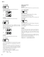
C-10   PB NAME

Confirm the proper connection, the name/ version of the plug-in board

through transmitting and receiving data between the unit and the plug-

in board, which is built in the unit.

Display of Test Results

OK:


NG:


Test End

The test result is displayed and the test will be finished.

Summary of Contents for Loopfactory AN200

Page 1: ...4 CIRCUIT BOARD LAYOUT 6 WIRING 6 BLOCK DIAGRAM 7 DISASSEMBLY PROCEDURE 8 LSI PIN DISCRIPTION 11 IC BLOCK DIAGRAM 15 DIMENSIONS 17 CIRCUIT BOARDS 18 TEST PROGRAM INITIALIZE 28 MIDI IMPLEMENTATION CHART 40 PARTS LIST OVERALL CIRCUIT DIAGRAM This document is printed on chlorine free ECF paper with soy ink 20010301 59800 ...

Page 2: ...of chemicals found by the California Health and Welfare Agency and possibly other entities to cause cancer and or birth defects or other reproductive harm DO NOT PLACE SOLDER ELECTRICAL ELECTRONIC OR PLASTIC COMPONENTS IN YOUR MOUTH FOR ANY REASON WHAT SO EVER Avoid prolonged unprotected contact between solder and your skin When soldering do not inhale solder fumes or expose eyes to solder flux va...

Page 3: ...ITCHES Sound Control Sw x 8 LFO Detail Key Assign VCO1 Wave Sync Mode VCO2 Wave Effect Type EG Select Dist Sw Scene x 2 Sequencer Sw x 2 Mode x 2 Pattern Select x 1 Keyboard Mode x 1 Step Select x 16 Step Group Select x 2 Track Select x 2 Play Effect x 2 Octave x 2 Tap Tempo x 1 Free EG Sw x 4 Free EG Mode x 1 Free EG Length x 1 Store x 1 Show Value x 1 Shift x 1 Exit x 1 4 DISPLAY 7SEG LED x 4 5 ...

Page 4: ...NG button PATTERN button DATA knob SHOW VALUE button STORE button EXIT button VOICE BLOCK SCENE group SCENE knob 1 button 2 button FREE EG group LENGTH button 1 button 2 button MODE button 3 button 4 button VOLUME knob LFO group DETAIL button SPEED knob EG group ATTACK knob DECAY knob SUSTAIN knob ...

Page 5: ...C PITCH knob NOISE LEVEL knob EFFECT group TYPE button PARAM PAN knob WET VOL knob VCF group CUTOFF TYPE knob RESONANCE knob FEG DEPTH knob CONTROL BLOCK 씰 START STOP button TAP button button SWING button REVERSE button SHIFT button OCT button OCT button KEYBOARD button PATTERN SELECT button SYNTH TRACK button RHYTHM TRACK button KEYBOARD BLOCK DC IN OUTPUT PHONES STAND BY ON MIDI IN MIDI OUT Rear...

Page 6: ...2 15P CN4 6P CN5 7P CN1 7P CN6 7P CN1 15P PLG LED DM PN 1 3 2 4 5 7 6 1 2 3 4 5 6 7 LOCATION KR KR DS KR DS KR KR KR DS KR PLG DM CONNECTOR NAME PIN LENGTH DESTINATION 16P L 80 7P L 450 4P L 380 15P L 220 7P L 150 6P L 200 15P L 50 PN CN1 DM CN2 DM CN6 DM CN3 DM CN1 DM CN4 DM CN5 LED CN1 PN CN5 PN CN3 PN CN2 PN CN6 PN CN4 PLG_AN CN1 ...

Page 7: ...onous Divider 3 3V Knob out Knob X 15 1 65V 3 3V Knob out Knob center click X 1 Panel SW With LED X 36 Panel SW X 15 Panel LED A0642 25 Panel Side CN1 3 3V LED DM PN PLG AN 2 1 3 4 5 6 7 8 9 10 11 12 13 14 15 16 TAP SWING REVERS OCT OCT TG TRACK SFX TRACK KEYBOARD PATTERN SELECT STEP 1 8 STEP 9 16 6P 6P 4P 4P 16P 16P 15P 15P 7P 7P 7P 7P 15P 15P IC6 IC6 IC11 IC11 IC16 IC19 IC10 IC5 IC5 IC5 IC5 IC8 ...

Page 8: ...bout 1 min 2 1 Remove the bottom assembly See Procedure 1 2 1 Remove the tree 3 screws marked 160 The PLG150 AN circuit board can then be removed Fig 2 Attachment consideration of the PLG150 AN circuit board When installing the PLG150 AN circuit board do with connector assembly as shown in the fig 2 1 Fit the PLG150 AN circuit board caring not to let the connector assembly in it 180 Bind Head Tapp...

Page 9: ...it is bent or broken Fig 2 2 DM PLG150 AN DM PLG Connector Assembly CN5 CN1 or OK NG SONG PATTERN STORE VELOCITY GATE TIME PITCH INST SEL BPM BEAT 210 200 200 PN 60 60 4 PN Circuit Board time required about 4 min 4 1 Remove the bottom assembly See Procedure 1 4 2 Remove the PLG150 AN circuit Board See Procedure 2 4 3 Remove the DM circuit Board See Procedure 3 4 4 Remove the seventeen 17 knobs mar...

Page 10: ...See Procedure 4 5 5 Remove the four 4 screws marked 40 The LED circuit board can then be removed Fig 5 LED 40 Battery VN103500 VN103600 Battery holder for VN103500 Notice for back up battery removal push the battery as shown in figure then the battery will pop up Druk de batterij neer beneden zoals aangeven in de tekening de batterij springt dan neer voren Battery Battery holder 40 Bind Head Tappi...

Page 11: ...bus Program address bus Power supply Ground Program address bus 85 86 87 88 89 90 91 92 93 94 95 96 97 98 99 100 101 102 103 104 105 106 107 108 109 110 111 112 113 114 115 116 117 118 119 120 121 122 123 124 125 126 127 128 129 130 131 132 133 134 135 136 137 138 139 140 141 142 143 144 145 146 147 148 149 150 151 152 153 154 155 156 157 158 159 160 161 162 163 164 165 166 167 168 CMA3 CMA8 CMA2 ...

Page 12: ...AC Serial output format select 81 82 83 84 85 86 87 88 89 90 91 92 93 94 95 96 97 98 99 100 101 102 103 104 105 106 107 108 109 110 111 112 113 114 115 116 117 118 119 120 121 122 123 124 125 126 127 128 129 130 131 132 133 134 135 136 137 138 139 140 141 142 143 144 145 146 147 148 149 150 151 152 153 154 155 156 157 158 159 160 SO7 SO6 SO5 VDD VSS SO4 SO3 SO2 SO1 SO0 WDCK SWPKON IRQN VDD VSS XTA...

Page 13: ...rt 6 Oout Stand by mode signal Reset Non maskable interrupt Ground Clock Clock Power supply Address strobe Read strobe Write strobe High Write strobe Low Mode select Analog power supply Reference voltage Analog data input EQ Analog input EQ Analog data input Analog input CS Analog data input BEND Analog input MOD Analog input FC Analog input BAT Analog ground Port 8 Chip select Ground Port A PA6 P...

Page 14: ... R output Analog power supply 9 10 11 12 13 14 15 16 O I I I I Channel R voltage reference Channel L voltage reference Channel L output Analog ground Word clock Channel R series input Series input Channel L series input Clock 4 8F D GND 16 BIT D VDD A GND R OUT A VDD A VDD R REF L REF L OUT A GND WDCK RSI SI LSI CLK UPD63200GS E1 XP867A00 DAC Digital to Analog Converter DM IC16 ...

Page 15: ...INPUTS OUTPUTS PR CLR CLK D Q Q L H H L H Q O H L H H L Q O X X X H L X X X X f f L H L L H H H L H L H H H 1 2 3 4 5 6 7 1CLR 1D 1CK 1PR 1Q 1Q GND 14 13 12 11 10 9 8 VCC 2CLR CLR 2D D 2CK CK 2PR PR 2Q 2Q Q Q CLR D CK PR Q Q DM IC14 IC25 HD74HC273FP XU533A00 MM74HC273SJX XY198A00 D FF 1 CLEAR 2 3 4 5 6 7 8 9 10 1Q 1D 2D 2Q 3Q 3D 4D 4Q GND 11 12 13 14 15 16 17 18 19 20 VCC 8Q 8D 7D 7Q 6Q 6D 5D 5Q C...

Page 16: ...verting Input A DC Voltage Supply DC Voltage Supply Output B Inverting Input B Non Inverting Input B Inverting Input A XR294A00 PN IC9 TC74HCT04AF T1 XI297A00 Hex Inverter 1 2 3 4 5 6 7 1A 1Y 2A 2Y 3A 3Y Vss 14 13 12 11 10 9 8 VDD 6A 6Y 5A 5Y 4A 4Y DM IC4 1 1A 2 3 4 5 6 7 1Y 2A 2Y 3A 3Y GND 8 9 10 11 12 13 14 VDD 6A 6Y 5A 5Y 4A 4Y MM74HC14JX XW104A00 Hex Inverter DM IC5 PLG150 AN IC9 TC74VHC14FT X...

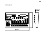
Page 17: ...17 AN200 DIMENSIONS 338 mm W 208 9 mm D 51 7 mm H SONG PITCH INST SEL PATTERN GATETIME BPM STORE VELOCITY BEAT ...

Page 18: ...e for back up battery removal push the battery as shown in figure then the battery will pop up Druk de batterij neer beneden zoals aangeven in de tekening de batterij springt dan neer voren Battery Battery holder PHONES OUTPUT L MONO R STAND BY ON DC IN IN OUT MIDI to PN CN5 to PLG150 AN CN1 to PN CN3 ...

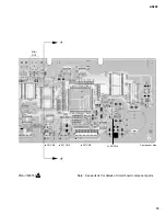
Page 19: ...19 AN200 MIDI OUT Component side 2NA V625760 2 Note See parts list for details of circuit board component parts to PN CN3 to PN CN4 to PN CN2 to PN CN6 ...

Page 20: ...20 AN200 DM CIRCUIT BOARD ...

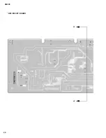
Page 21: ...21 AN200 Pattern side 2NA V625760 2 ...

Page 22: ...DM CN6 to DM CN3 to DM CN4 DATA PATTERN SONG SHCW VALUE STORE EXIT 씰 TAP SWING REVERSE SHIFT OCT OCT KEYBOARD PATTERN SELECT RHYTHM TRACK SYNTH TRACK 1 2 3 STEP 1 8 STEP 9 16 1 2 3 9 10 11 SPEED ATTACK DETAIL POLY MONO UNISON KEYASGN PORTAMENTO VCO 1 2 SAW PULSE MIX VARI MLTSAW MODE FM DEPTH WAVE ...

Page 23: ...to DM CN4 ATTACK FM DEPTH MODE 3 11 4 5 12 13 6 7 8 14 15 16 SYNC PITCH NOISE LEVEL RESONANCE FEG DEPTH OFF VCO1 VCO2 SAW PULSE MIX TRI SINE TYPE CUTOFF TYPE PARAM PAN WET VOC DECAY FLGR RFSR OD AMP DECAY SUSTAIN RELEASE SELECT FEG AEG SWITH SCENE 1 2 LENGTH 1 2 3 4 MODE VOLUME to DM CN2 to DM CN1 WAVE ...

Page 24: ...24 AN200 PN CIRCUIT BOARD ...

Page 25: ...25 AN200 Pattern side 2NA V488620 Note See parts list for details of circuit board component parts to LED CN1 ...

Page 26: ...26 AN200 Component side Note See parts list for details of circuit board component parts PLG150 AN Circut Board Pattern side 2NA V414740 to DM CN5 N C ...

Page 27: ...27 AN200 LED CIRCUIT BOARD Component side 2NA V488650 Note See parts list for details of circuit board component parts SONG PATTERN STORE PIT CH GATE TIME VELOCITY INST SEL BPM BEAT to PN CN1 ...

Page 28: ... on the soldered surface of the DM circuit board is from 2 9 V up to 3 4 V during the power standby mode Start up of the test program While pressing the SHOW VALUE STORE and EXIT keys turn on the STANDBY switch Proceeding through the test program When the test program is started first TEST will appear on the LED display for about one second and then the test program version and the test number wil...

Page 29: ...0 2dBm load 10k Ω 5 0 2dBm load 10k Ω C 14 Factory set C 15 EXIT Reverberated noise level OUTPUT L OUTPUT R less than 88 dBm C 16 OK NG C 1 CPU RAM This is the read write verify check for the MAIN CPU RAM Display of Test Results OK NG Test End The test result is displayed and the test will be finished Refer to The test procedure when an error is detected when NG No Good error is detected C 2 RAM B...

Page 30: ...hen all switches are checked normally the OK is displayed and the test will be finished C 4 DATA ENTRY Rotate slowly the knob for DATA ENTRY clockwise until the value 23 appears on the LED display When 23 appears a sine wave sounds After this rotate slowly the knob counterclockwise to confirm that a sine wave sounds again and the OK is displayed on the LED when the value becomes 0 zero Display of ...

Page 31: ...n 80dBm load 10k Ω PHONES L 4 0 2 dBm load 33 Ω ADistortion less than 0 6 PHONES R less than 60dBm load 33 Ω Display of Test Results Not appearing Test End Rotate DATA ENTRY knob clockwise to proceed to the next test C 9 1kHz OUTPUT R Insert the appropriate phone plugs into each output jack of the OUT PUT L R and PHONE L R and then connect them to a fre quency counter oscilloscope and AC volt mete...

Page 32: ...re output from OUTPUT L Frequency 1kHz 3Hz Level 2 0dBm 2dBm Display of Test Results Not appearing Test End Rotate DATA ENTRY knob clockwise to proceed to the next test C 14 FACTORY SET This test is used to initialize the data to the factory settings Following operation will execute the test Press STORE to execute the factory settings Press EXIT to indicate the LCD display where you can select the...

Page 33: ... when too much MIDI data has been received at one time causing the unit to stop processing data This appears when the received MIDI data is incorrect or contains errors This appears when checksum of the received System Exclusive data is incorrect Err1 Err1 Err1 Err1 Err1 flashes Err2 Err2 Err2 Err2 Err2 flashes Err3 Err3 Err3 Err3 Err3 flashes Err4 Err4 Err4 Err4 Err4 flashes Battery Low MIDI Buff...

Page 34: ...34 AN200 ...

Page 35: ...35 AN200 ...

Page 36: ...36 AN200 ...

Page 37: ...37 AN200 ...

Page 38: ...38 AN200 ...

Page 39: ...39 AN200 ...

Page 40: ...6 38 o o Data Entry Control 64 65 x o 71 75 o o Sound Controller Change 94 o o Effect Depth 98 99 o o NRPN LSB MSB 16 18 19 80 83 o o Knob Control Prog o o 0 127 Change True 0 127 System Exclusive o o Song Pos o 3 o 2 Common Song Sel x x Tune x x System Clock o 3 o 4 Real Time Commands o 3 o 2 Aux All Sound off x o 120 126 127 Reset All Cntrls x o 121 Local ON OFF x x All Notes OFF x o 123 125 Mes...

Page 41: ...ort model 110V H North European model W General export model 220V I Indonesian model N X General export model J Japanese model Y Export model WARNING Components having special characteristics are marked and must be replaced with parts having specifications equal to those originally installed The numbers in QTY shows quantities for each unit The parts with in Part No are not available as spare part...

Page 42: ...2 AN200 OVERALL ASSEMBLY 30 20 210 200 220 150 130 140 160 120 185 180 110 100 10a 10b 40 60 80 70 90 170b 170a Bottom Assembly 170 PN Assembly See page 4 50 Upper Case Assembly 10 ...

Page 43: ...rcuit Board JK Terminal DM Terminal Lithium Battery Bind Head Tapping Screw P Angle L Angle R Circuit Board Bind Head Tapping Screw B Bottom Assembly Foot Bind Head Tapping Screw B Bind Head Tapping Screw B Knob Knob Knob Power Switch ACCESSORIES AC Adapter AC Adapter AC Adapter CD ROM LM DE 500 8mm J 2 6X8 MFZN2Y DE 2 6X8 MFZN2Y S 34Z BK 1 16P 80mm P 1 0 12X50 J CR2032 2 6X8 MFZN2Y PLG150 AN 3 0X...

Page 44: ...V6776500 V6776600 V6747300 V6747400 VP834600 PN ASSEMBLY PN Assembly Circuit Board Button Button Button Button Button Adhesive Tape Connector Assembly Connector Assembly DE J M1B MR1B MR2B 3B 2B 12X50 7P KR KR 450L 7P KR KR 150L AN200 V679220 LENGHT MODE DETAIL KEY ASGN WAVE MODE WAVE TYPE SELECT 1 2 SWITCH 1 2 3 4 SHOW VALUE STORE EXIT SONG PATTERN V677500 V677510 9 3 2 01 02 ...

Page 45: ...c Capacitor B chip Ceramic Capacitor F chip Electrolytic Cap chip Electrolytic Cap chip Electrolytic Cap chip Ceramic Capacitor SL chip Ceramic Capacitor SL chip Ceramic Capacitor F chip Ceramic Capacitor B chip Electrolytic Cap chip Ceramic Capacitor B chip Electrolytic Cap chip Ceramic Capacitor B chip Ceramic Capacitor B chip Electrolytic Cap chip Ceramic Capacitor B chip Ceramic Capacitor B ch...

Page 46: ...c Capacitor B chip Ceramic Capacitor B chip Ceramic Capacitor B chip Ceramic Capacitor B chip Electrolytic Cap chip Ceramic Capacitor B chip Ceramic Capacitor B chip Ceramic Capacitor B chip Ceramic Capacitor B chip Ceramic Capacitor F chip Ceramic Capacitor F chip Ceramic Capacitor B chip Ceramic Capacitor F chip Ceramic Capacitor F chip Ceramic Capacitor B chip Ceramic Capacitor B chip Ceramic C...

Page 47: ...e Chip Inductance Chip Inductance Chip Inductance Chip Inductance Chip Inductance Coil Chip Inductance Chip Inductance Chip Inductance Chip Inductance NFM4516P13C204FT1 STF 104ZB TBM NFM4516P13C204FT1 NFM4516P13C204FT1 STF 104ZB TBM STF 104ZB TBM STF 104ZB TBM PC410T HCPL M600 UPC2909T E1 SI 8050S LF1103 TC74HCT04AF T1 MM74HC14SJX M5216FP 600C NJM4556AMT1 SN74HC157NSR MM74HC157SJX TC7S66F M62021FP...

Page 48: ...or Array Resistor Array Resistor Array Resistor Array Resistor Array Resistor Array Resistor Array Resistor Array Resistor Array Resistor Array Resistor Array Resistor Array Resistor Array Resistor Array Resistor Array Resistor Array Resistor Array Resistor Array Resistor Array Carbon Resistor chip Carbon Resistor chip Carbon Resistor chip Carbon Resistor chip Carbon Resistor chip Carbon Resistor ...

Page 49: ...bon Resistor chip Carbon Resistor chip Carbon Resistor chip Carbon Resistor chip Carbon Resistor chip Carbon Resistor chip Carbon Resistor chip Carbon Resistor chip Carbon Resistor chip Carbon Resistor chip Carbon Resistor chip Carbon Resistor chip Carbon Resistor chip Carbon Resistor chip Carbon Resistor chip Carbon Resistor chip Carbon Resistor chip Carbon Resistor chip Carbon Resistor chip Carb...

Page 50: ...r F chip Ceramic Capacitor F chip Ceramic Capacitor F chip Ceramic Capacitor F chip Ceramic Capacitor F chip Ceramic Capacitor F chip Ceramic Capacitor F chip Ceramic Capacitor F chip Ceramic Capacitor F chip Electrolytic Cap chip Ceramic Capacitor F chip Ceramic Capacitor F chip Ceramic Capacitor F chip Ceramic Capacitor F chip Ceramic Capacitor F chip Ceramic Capacitor F chip Ceramic Capacitor F...

Page 51: ...ode Diode Diode Diode Diode Diode Diode Diode Diode Diode Diode Diode Diode Diode Diode Diode Diode Diode Diode Diode Diode Diode Diode Diode Diode Diode Diode Diode Diode Diode Diode Diode Diode Diode Diode Diode Diode Diode Diode Diode Diode Diode Diode Diode Diode Diode Rotary Encoder IC IC IC IC IC IC IC 0 0100 50V K 0 0100 50V K 0 0100 50V K 0 0100 50V K 0 0100 50V K 0 0100 50V K 0 0100 50V K...

Page 52: ...D LED LED LED LED LED LED LED LED LED LED LED LED LED HD74HC273FP MM74HC273SJX HD74HC273FP MM74HC273SJX HD74HC273FP MM74HC273SJX HD74HC4051FPEL TC74HC4051AFEL HD74HC4051FPEL TC74HC4051AFEL NJM3414AM T1 TLOU1008 TLOU1008 TLOU1008 TLOU1008 TLOU1008 TLOU1008 TLOU1008 TLOU1008 TLOU1008 TLOU1008 TLOU1008 LN282RPX RED LN282RPX RED LN282RPX RED TLOU1008 TLOU1008 LN282RPX TX3 RED LN282RPX TX3 RED LN282RPX...

Page 53: ...ip Carbon Resistor chip Carbon Resistor chip Carbon Resistor chip Carbon Resistor chip Carbon Resistor chip Carbon Resistor chip Carbon Resistor chip Carbon Resistor chip Carbon Resistor chip Carbon Resistor chip Carbon Resistor chip Carbon Resistor chip Carbon Resistor chip Tact Switch Tact Switch Tact Switch Tact Switch Tact Switch Tact Switch Tact Switch Tact Switch Tact Switch Tact Switch Tact...

Page 54: ...Ceramic Cap Electrolytic Cap chip Electrolytic Cap chip Electrolytic Cap chip Monolithic Ceramic Cap Electrolytic Cap chip Carbon Resistor chip Carbon Resistor chip Carbon Resistor chip Carbon Resistor chip Carbon Resistor chip Carbon Resistor chip Carbon Resistor chip Carbon Resistor chip Monolithic Ceramic Cap Monolithic Ceramic Cap Monolithic Ceramic Cap Monolithic Ceramic Cap Monolithic Cerami...

Page 55: ...Resistor chip Carbon Resistor chip Carbon Resistor chip Carbon Resistor chip Carbon Resistor chip Carbon Resistor chip Carbon Resistor chip Resistor Array Resistor Array Resistor Array Resistor Array Resistor Array Rubber Contact Connector Assembly AC Adapter AC Adapter AC Adapter SDM4260CLU 6S MSM514260C 60JS SDM4260CLU 6S TC74VHC153FT TC74VHC14FT HD74LV14AT TC74VHC245FT HD74LV245AT TC74VHC139FT ...

Page 56: ...ack up battery removal push the battery as shown in figure then the battery will pop up Druk de batterij neer beneden zoals aangeven in de tekening de batterij springt dan neer voren Battery Battery holder Note See parts list for details of circuit board component parts AN200 DM BATTERY SOCKET SWX00B OP AMP OP AMP DAC REGURATOR 5V OP AMP OP AMP MULTIPLEXER TRANSCEIVER INVERTER D FF D FF REGURATOR ...

Page 57: ...200 OVERALL CIRCUIT DIAGRAM 2 3 PN LED PN 28CCI 8818206 LED 28CCI 8818207 AN200 AN200 Note See parts list for details of circuit board component parts AN200 PN LED D FF D FF D FF D FF D FF TRANSCEIVER MUL TIPLEXER MUL TIPLEXER OP AMP to DM CN3 to DM CN4 to DM CN6 to DM CN2 to DM CN1 ...

Page 58: ... AN200 AN200 OVERALL CIRCUIT DIAGRAM 3 3 PLG150 AN FRASH ROM 8M MASK ROM 8M 16M DRAM 4M INVERTER INVERTER MDSP DECODER PLG150 AN CPU VOP3 MULTIPLEXER DRAM 4M INVERTER INVERTER BUFFER not installed to DM CN5 28CA2 8814155 ...

Reviews: