PSR540
9
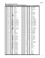
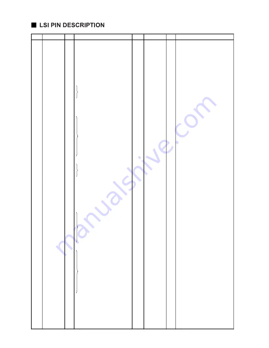
HG73C205AFD (XU947C00) SWX00B TONE GENERATOR
PIN
NO.
NAME
I/O
FUNCTION
PIN
NO.
NAME
I/O
FUNCTION
1
ICN
I
Initial clear
85
CMA3
O
Program address bus
2
RFCLKI
I
PLL Clock
86
CMA8
O
Program address bus
3
TM2
I
PLL Control
87
CMA2
O
Program address bus
4
AVDD_PLL
Power supply
88
CRD
O
read signal
5
AVSS_PLL
Ground
89
CMA1
O
Program address bus
6
MODE0
I
SWX dual mode
90
CUB
O
high byte effective signal
7
VCC7
Power supply
91
VCC91
Power supply
8
GND8
Ground
92
GHND92
Ground
9
XIN
I
crystal oscillator
93
CS1
O
CS signal
10
XOUT
O
crystal oscillator
94
CMA0
O
Program address bus
11
MODE1
I
SWX separate mode
95
CLB
O
low byte effective signal
12
TEST0
I
TEST pin
96
CMA12
O
Program address bus
13
TESTON
I
TEST pin
97
CMA11
O
Program address bus
14
AN0-P40
I
A/D converter
98
CMA10
O
Program address bus
15
AN1-P41
I
A/D converter
99
CMA9
O
Program address bus
16
AN2-P42
I
A/D converter
100
GND100
Ground
17
AN3-P43
I
A/D converter
101
CWE
O
write signal
18
AVDD_AN
Power supply
102
CMA16
O
Program address bus
19
AVSS_AN
Ground
103
CMA15
O
Program address bus
20
TXD0
O
for MIDI or TO-HOST
104
CMA14
O
Program address bus
21
TXD1
O
for MIDI
105
CMA13
O
Program address bus
22
EXCLK
I
Crystal oscillator
106
CMD8
I/O
Program memory Data bus
23
SMD11
I/O
Wave memory data bus
107
CMD7
I/O
Program memory Data bus
24
SMD4
I/O
Wave memory data bus
108
CMD9
I/O
Program memory Data bus
25
SMD3
I/O
Wave memory data bus
109
CMD6
I/O
Program memory Data bus
26
SMD12
I/O
Wave memory data bus
110
CMD10
I/O
Program memory Data bus
27
SMD10
I/O
Wave memory data bus
111
CMD5
I/O
Program memory Data bus
28
SMD5
I/O
Wave memory data bus
112
CMD11
I/O
Program memory Data bus
29
SMD2
I/O
Wave memory data bus
113
CMD4
I/O
Program memory Data bus
30
SMD13
I/O
Wave memory data bus
114
CMD12
I/O
Program memory Data bus
31
SMD9
I/O
Wave memory data bus
115
CMD3
I/O
Program memory Data bus
32
SMD6
I/O
Wave memory data bus
116
CMD13
I/O
Program memory Data bus
33
SMD1
I/O
Wave memory data bus
117
CMD2
I/O
Program memory Data bus
34
SMD14
I/O
Wave memory data bus
118
CMD14
I/O
Program memory Data bus
35
VCC35
Power supply
119
VCC119
Power supply
36
GND36
Ground
120
GND115
Ground
37
SMD8
I/O
Wave memory data bus
121
CMD1
I/O
Program memory Data bus
38
SMD7
I/O
Wave memory data bus
122
CMD15
I/O
Program memory Data bus
39
SMD0
I/O
Wave memory data bus
123
CMD0
I/O
Program memory Data bus
40
SMD15
I/O
Wave memory data bus
124
CMA21
O
Program address bus
41
SOE
O
read signal
125
PDT15
I/O
SWX access data bus
42
SWE
O
write signal
126
PDT14
I/O
SWX access data bus
43
SRAS
O
RAS signal
127
PDT13
I/O
SWX access data bus
44
SCAS
O
CAS signal
128
PDT12
I/O
SWX access data bus
45
REFRESH
O
REFRESH signal
129
PDT11
I/O
SWX access data bus
46
CS0
O
CS signal
130
PDT10
I/O
SWX access data bus
47
SMA0
O
Memory address bus
131
PDT9
I/O
SWX access data bus
48
SMA16
O
Memory address bus
132
PDT8
I/O
SWX access data bus
49
VCC49
Power supply
133
VCC133
Power supply
50
GND50
Ground
134
GND134
Ground
51
SMA1
O
Memory address bus
135
PDT7
I/O
SWX access data bus
52
SMA15
O
Memory address bus
136
PDT6
I/O
SWX access data bus
53
SMA2
O
Memory address bus
137
PDT5
I/O
SWX access data bus
54
SMA14
O
Memory address bus
138
PDT4
I/O
SWX access data bus
55
SMA3
O
Memory address bus
139
PDT3
I/O
SWX access data bus
56
SMA13
O
Memory address bus
140
PDT2
I/O
SWX access data bus
57
SMA4
O
Memory address bus
141
PDT1
I/O
SWX access data bus
58
SMA12
O
Memory address bus
142
PDT0
I/O
SWX access data bus
59
SMA5
O
Memory address bus
143
VCA143
Power supply
60
GND60
Ground
144
GND144
Ground
61
VCC61
Power supply
145
PAD2
I
SWX access address bus
62
SMA11
O
Memory address bus
146
PAD1
I
SWX access address bus
63
SMA6
O
Memory address bus
147
PAD0
I
SWX access address bus
64
SMA10
O
Memory address bus
148
VCC148
Power supply
65
SMA7
O
Memory address bus
149
GND149
Ground
66
SMA9
O
Memory address bus
150
PCS
I
Chip select
67
SMA17
O
Memory address bus
151
PWR
I
write enable
68
SMA8
O
Memory address bus
152
PRD
I
read enable
69
SMA18
O
Memory address bus
153
RXD0
I
for Midi or TO-HOST
70
SMA19
O
Memory address bus
154
RXD1
I
for Midi or Key scan
71
SMA20
O
Memory address bus
155
SCLKI
I
EXT Clock
72
SMA21
O
Memory address bus
156
ADIN
I
A/D converter
73
SMA22
O
Memory address bus
157
ADLR
O
A/D converter LR clock
74
SMA23
O
Memory address bus
158
DO0
O
DAC
75
CMA20
O
Program address bus
159
DO1
O
DAC
76
CMA19
O
Program address bus
160
SYSCLK
O
1/2 clock
77
VCC77
Power supply
161
VCC161
Power supply
78
GND78
O
Ground
162
GND162
Ground
79
CMA18
O
Program address bus
163
WCLK
O
for DAC LR clock
80
CMA17
O
Program address bus
164
QCLK
O
1/12 clock
81
CMA5
O
Program address bus
165
BCLK
O
IIS-DAC clock
82
CMA6
O
Program address bus
166
SYI
I
Synch signal
83
CMA4
O
Program address bus
167
IRQ0
I
Interrupt request
84
CMA7
O
Program address bus
168
NMI
I
Interrupt request
(DM IC200)


