background image

37

RX-V365/HTR-6230

RX-V365/HTR-6230

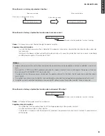
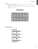
1 1 . B T   C L R : I N H I

I 4 . B T   C L R : R S R V

1 2 .

1 3 . P R E S E T   I N H I

1 3 . P R E S E T   R S R V

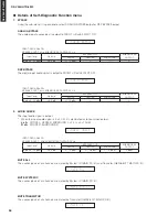
Preset Group

P1

P2

P3

P4

P5

P6

P7

P8

A

B

C

D

E

Initialization inhibited

Initialization reserved

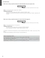
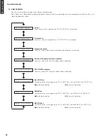
12. NO MENU

13. FACTORY PRESET

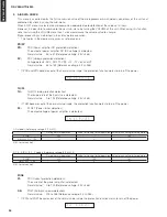
This menu is used to reserve and inhibit initialization of the back-up IC.
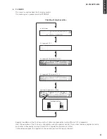
The signals are processed using EFFECT OFF (The L/R signal is output using ANALOG BYPASS).

CAUTION: 

Before setting to the PRESET RESERVED, write down the existing preset memory content of the tuner in a 
table as shown below.
(This is because setting to the PRESET RESERVED will cause the user memory content of the tuner to be 
erased.)

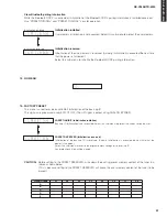
PRESET INHIBIT (Initialization inhibited)

Back-up IC initialization is not executed. Select this sub-menu to protect the values set by the user.

PRESET RESERVED (Initialization reserved)

Initialization of the back-up IC is reserved. (Actually, initialization is executed the next time that the 
power is turned on.)
Select this sub-menu to reset to the original factory settings or to reset the IC.
Any protection history will be cleared.

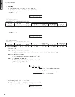
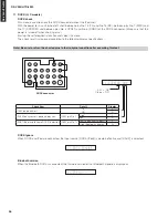
Clear Bluetooth pairing information

While the Bluetooth DOCK is connected, initialization of the Bluetooth DOCK pairing information is inhibited/reserved.
Use “PRESET/TUNING<” and “PRESET TUNING>” keys for operation.

Initialization inhibited

User memory initialization is not executed. Select this sub-menu to protect the user memory.

Initialization reserved

Initialization of the use memory is reserved. (Actually, initialization is executed the next time 
that the power is turned on.)
Select this sub-menu to initialize the Bluetooth DOCK pairing information.

Summary of Contents for RX-V365

Page 1: ...ineering and service departments of YAMAHA are continually striving to improve YAMAHA products Modifications are therefore inevitable and specifications are subject to change without notice or obligat...

Page 2: ...rom supply circuits Meter impedance should be equivalent to 1500 ohms shunted by 0 15 F All of the P C B s installed in this unit and solder joints are soldered using the lead free solder Among some t...

Page 3: ...3 RX V365 HTR 6230 RX V365 HTR 6230 FRONT PANELS Top view Front view RX V365 R K A B G E F L models RX V365 U C models RX V365 T model...

Page 4: ...4 RX V365 HTR 6230 RX V365 HTR 6230 HTR 6230 U C models HTR 6230 T model HTR 6230 R K G E F models...

Page 5: ...5 RX V365 HTR 6230 RX V365 HTR 6230 Nameplate REAR PANELS RX V365 U C models RX V365 R model RX V365 T model...

Page 6: ...6 RX V365 HTR 6230 RX V365 HTR 6230 RX V365 A model RX V365 B G E F models RX V365 K model...

Page 7: ...7 RX V365 HTR 6230 RX V365 HTR 6230 HTR 6230 U C models HTR 6230 R model RX V365 L model...

Page 8: ...8 RX V365 HTR 6230 RX V365 HTR 6230 HTR 6230 T model HTR 6230 K model HTR 6230 G E F models...

Page 9: ...9 RX V365 HTR 6230 RX V365 HTR 6230 REMOTE CONTROL PANELS T model RAV283 U C models RAV284 R T K A L models RAV34 B G E F models...

Page 10: ...on 1 kHz 50 W CD etc 2 ch STEREO to FRONT L R SP OUT U C models 8 ohms 0 06 or less R T K A B G E F L models 6 ohms 0 06 or less Signal to Noise Ratio IHF A Network CD etc STEREO Input shorted to SP O...

Page 11: ...ries Remote control x 1 Batteries R03 AAA UM 4 x 2 Indoor FM antenna x 1 AM loop antenna x 1 Optimizer microphone x 1 R K A B G E F L models Sheet x 1 T model Specifications are subject to change with...

Page 12: ...SYSTEM O O CD Music Listening CD STEREO 2ch Stereo SYSTEM O O Radio Listening TUNER RADIO FM AM FM AM TUNER MUSIC ENHANCER Music Enh 5ch SYSTEM O SCENE 4 O SCENE 4 DOCK Listening DAP iPod DOCK V AUX M...

Page 13: ...SWFR C SP DISTANCE UNIT feet feet ft meters m FRONT L 10 0 ft feet 1 0 to 80 0 ft 10 0 ft 0 5 ft step FRONT R 10 0 ft CENTER 8 5 ft feet 1 0 to 80 0 ft 8 5 ft 0 5 ft step SUR L 8 0 ft feet 1 0 to 80...

Page 14: ...a to z Figure 0 to 9 Space Marks C VOLUME TRIM CD TUNER MD CD R DVD DTV CBL V AUX DOCK U C models DVR MULTI CH INPUT 6 0 to 6 0 dB 0 0 dB 1 0 dB step D DECODER MODE AUTO LAST CD DVD DTV CBL AUTO DTS E...

Page 15: ...dels MAIN 3 P C B AM FM TUNER HDMI P C B OPERATION 4 P C B DSP P C B MAIN 4 P C B MAIN 1 P C B OPERATION 2 P C B OPERATION 11 P C B OPERATION 10 P C B OPERATION 6 P C B OPERATION 1 P C B OPERATION 7 P...

Page 16: ...der as numbered Disconnect the power cable from the AC outlet 1 Removal of Top Cover a Remove 4 screws 4 screws and screw Fig 1 b Slide the top cover rearward to remove it Fig 1 2 Removal of Front Pan...

Page 17: ...CB905 Fig 2 b Remove 5 screws Fig 3 c Remove the HDMI P C B Fig 2 4 Removal of OPERATION 4 P C B a Remove CB181 182 and CB193 Fig 2 b Remove 7 screws Fig 3 c Remove the OPERATION 4 P C B Fig 2 5 Remov...

Page 18: ...ing the P C B a Remove the top cover Fig 1 b Remove 3 screws Fig 3 c Remove 5 screws and 4 screws Fig 4 d Place the P C B s with rear panel upright Fig 5 e Connect the ground of heat sink rear panel a...

Page 19: ...write the latest firmware DSP P C B IC201 DSP P C B Required tools DVD or CD player with DIGITAL OUTPUT OPTICAL or COAXIAL jack Optical cable when OPTICAL jack is used Digital audio pin cable when CO...

Page 20: ...e STANDBY ON and SPEAKERS keys of this unit connect the power cable of this unit to the AC outlet Fig 2 The FIRMWARE UPDATE mode is activated and SPDIF Upgrade is displayed Fig 2 2 Connect the power c...

Page 21: ...en the disc tray 10 Remove the firmware CD from the disc tray and close the disc tray 11 Press the STANDBY ON key of the DVD CD player to turn off the power 12 Press the STANDBY ON key of this unit to...

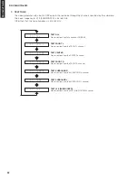
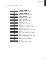
Page 22: ...RN 7 TEST TONE TEST ALL TEST FRONT L TEST CENTER TEST FRONT R TEST SURR R TEST SURR L TEST LFE 8 PROTECTION PRD L xxx PRD H xxx PRV L xxx PRV H xxx THM xxx PLDET8_L xxx PLDET8_H xxx PLDET6_L xxx PLDET...

Page 23: ...History 3 History 4 11 DOCK DOCK xxx DOCK ignore BTYS xxx BT CLR RSRV 12 NO MENU Not applied to these models 13 FACTORY PRESET PRESET INHI PRESET RSRV 14 ROM VER SUM TOTAL VERSION CRC14 ALL program C...

Page 24: ...FL display of this unit flashes to indicate that the mode is self diagnostic function mode with the protection functions disabled Canceling Self Diagnostic Function 1 Before canceling self diagnostic...

Page 25: ...hould be checked for damage before applying power to this unit Amplifier current should be monitored by measuring DC voltage across the emitter resistors for each channel When there is a history of pr...

Page 26: ...heat sink is excessive Supplementary information The protection function worked due to the temperature limit being exceeded Causes could be poor ventilation or a defect related to the thermal sensor I...

Page 27: ...gnostic Function mode In addition to the self diagnostic function menu items functions as listed below are available Power on off Master volume Muting Speakers A B OFF Input selection Tone control Fun...

Page 28: ...UT 1 kHz SUBWOOFER OUTPUT 50 Hz Details of Self Diagnostic Function menu 1 BYPASS Using the sub menu it is possible to select ANALOG BYPASS output or DSP BYPASS output ANALOG BYPASS The analog input a...

Page 29: ...specified by LFE BASS CENTER NONE The CENTER signal is distributed to FRONT L R LFE BASS FRONT The LFE SUBWOOFER signal is distributed to FRONT L R TONE MAX The signal is output with the tone control...

Page 30: ...kHz SUBWOOFER OUTPUT 50 Hz 4 6CH INPUT The input source MULTI CHANNEL INPUT is selected It is possible to select the 6 ohm 8 ohm by using the sub menu 6 ch INPUT 6 ohm 6 ch INPUT 8 ohm LIM PLDET THM L...

Page 31: ...to check the FL display section The audio signal is processed using STRAIGHT Segment conditions of the FL driver and the FL tube are checked by turning ON and OFF all segments Next the operation of th...

Page 32: ...oise frequency for LFE SUBWOOFER is 35 to 80 Hz Other than that the noise frequency is 500 to 2 kHz TEST ALL Noise is output from all channels LFE BASS TEST FRONT L Noise is output from the FRONT L ch...

Page 33: ...isplayed PRV Voltage protection High The maximum preset value of PRV is displayed THM Thermo protection High The maximum preset value of THM is displayed PLD PLDET Power limiter detection 8 ohm Low Th...

Page 34: ...ange Signal processing is maintained in the status before execution The figures in the diagram are given as reference only PD PV PD PRD Power amplifier DC protection detection The output of power ampl...

Page 35: ...P R I 9 0 1 0 P R D 0 1 0 T H M 2 5 5 1 0 N O P R O T Example Example Example Example K0 K1 K0 K1 KEY0 KEY1 Panel key of this unit When the A D conversion value of the panel key becomes out of the spe...

Page 36: ...self With the power to this unit turned off short between pins No 14 TX and No 18 RX between pins No 1 PWR and No 17 ACCPOW and between pins No 4 iPDET and No 8 DGND of the DOCK connector Make sure th...

Page 37: ...ialization is not executed Select this sub menu to protect the values set by the user PRESET RESERVED Initialization reserved Initialization of the back up IC is reserved Actually initialization is ex...

Page 38: ...roprocessor IC101 DSP P C B is displayed Program checksum Checksum value of application and standby code program is displayed SPI Serial Peripheral Interface checksum Checksum value of SPI firmware up...

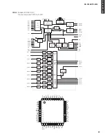
Page 39: ...23 NX 22 NX 21 17G 20 16G 19 15G 18 14G 17 13G 16 12G 15 11G 14 10G 13 9G 12 8G 11 7G 10 6G 9 5G 8 4G 7 3G 6 2G 5 1G 4 NP 3 NP 36 P30 35 P31 2 1 F1 NX Connection PIN CONNECTION GRID ASSIGNMENT 2G 1G...

Page 40: ...a 1b 1c 1d 1e 1f 1g 2a 2b 2c 2d 2e 2f 2g S23 S24 S25 S13 S14 16G S1 S6 S7 S8 S9 S10 S11 S12 S20 S21 13G 1G 1 1 2 1 3 1 4 1 5 1 1 2 2 2 3 2 4 2 5 2 1 3 2 3 3 3 4 3 5 3 1 4 2 4 3 4 4 4 5 4 1 5 2 5 3 5 4...

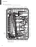
Page 41: ...6 ADDR17 ADDR18 ADDR19 BGH BG VDDEXT GND DATA0 DATA1 DATA2 DATA3 DATA4 VDDINT DATA5 DATA6 DATA7 VDDEXT GND DATA8 DATA9 DATA10 DATA11 DATA12 DATA13 DATA14 DATA15 GND BMODE0 BMODE1 TCK VDDEXT GND GND GN...

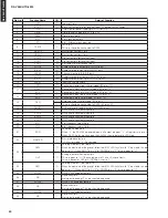
Page 42: ...VDDEXT VDDEXT I O power supply EX3 3 32 ICXM PF12 O 33 XMPWR PF11 O 34 INTAK PF10 I CODEC IC IC301 interrupt 35 FSYNC TFS0 PF9 I Frame sync detect 36 R2A_DATA PF8 O DATA for R2A volume selector IC IC...

Page 43: ...iter control output 80 VDDINT VDDINT Power supply of microprocessor BF1 2 81 DTXM TX O 82 DRXM RX I 83 EMU O 84 TRST I 85 TMS I 86 TDI I 87 TDO O 88 DGND GND Ground of external 89 DGND GND Ground of e...

Page 44: ...Ground of external 145 VDDEXT VDDEXT I O power supply EX3 3 146 A04 ADDR4 O SDRAM address bus 04 147 A03 ADDR3 O SDRAM address bus 03 148 A02 ADDR2 O SDRAM address bus 02 149 A01 ADDR1 O SDRAM address...

Page 45: ...DC input select 2 14 6Q ADSEL1 4ch ADC input select 1 15 5Q ADSEL0 4ch ADC input select 0 16 4Q CCBE SPI bus switch 17 3Q CMT Center mute 18 2Q SMT Surround mute 19 1Q FMT Front mute 20 VCC EX3 3 Powe...

Page 46: ...7D D06 Data bus 06 9 8D D07 Data bus 07 10 GND DGND Ground of external 11 LE LEEX2 Bank select 2 12 8Q VR1 Video select R 13 7Q SPISEL5 CE for tuner 14 6Q 8ohmSW AC H L relay RY106 MAIN P C B 15 5Q HP...

Page 47: ...DC select port IC402 IC403 SN74LV4051APWR DSP P C B 8 channel analog multiplexers demultiplexers Key input A D pull up resistance 10 k ohms Pin No Port Name Function Name Detail of Function 1 CS SPISE...

Page 48: ...on Name Detail of Function 1 Y4 DEST Destination 1 2 Y6 PDET Sub trans detect 3 COM COM SPI bus IN3 IC401 4 Y7 HP Headphone detect 5 Y5 PRIIN Current protection 6 INH DGND Pull down 7 GND DGND Ground...

Page 49: ...UT4 ROUT4 DAC DATT DEM DAC DATT DEM DAC DATT DEM DAC DATT DEM DAC DATT DEM DAC DATT DEM DAC DATT DEM AVDD AVSS CCLK SCL CDTI SDA CSN DAUX1 SDTI4 SDTI3 SDTI2 SDTI1 XTL1 XTL0 PDN MASTER DZF2 DZF1 LOUT4...

Page 50: ...I This pin should be connected to DVSS I2C pin H 24 DAUX1 I AUX audio serial data input pin ADC DAC part 25 SDTI4 I DAC4 audio serial data input pin 26 SDTI3 I DAC3 audio serial data input pin 27 SDTI...

Page 51: ...61 RX2 I Receiver channel 2 pin Internal biased pin Internally biased at PVDD 2 62 NC No connect pin No internal bonding This pin should be connected to PVSS 63 RX3 I Receiver channel 3 pin Internal b...

Page 52: ...SBR OUT SBL OUT SBLC SBRC SWC SRC SLC A GND A GND A GND A GND A GND A GND TREL BASSL2 BASSL1 82 83 84 85 86 87 88 89 90 91 92 93 94 95 96 97 98 99 100 50 A VEE 0 6 12 18dB ATT SUB 0 95dB 0 5dBstep SUB...

Page 53: ...SR SBL SBR ch terminal to connect capacitor to reduce noise from changing the volume 25 N C No connected 26 BASSL1 L R ch tone control Bass terminal for setting frequency characteristics 27 BASSL2 L...

Page 54: ...ch input terminal input selector 79 INL9 L R ch input terminal input selector 80 N C No connected 81 INRB RECR2 L R ch input terminal input selector L R ch REC output terminal 82 INLB RECL2 L R ch in...

Page 55: ...t 31 SEG13 P22 Segment output 32 SEG12 P23 Segment output Connect to segment anode pins of VFD 33 SEG11 P24 Segment output 34 SEG10 P25 Segment output 35 SEG09 P26 Segment output 36 SEG08 P27 Segment...

Page 56: ...D DTV CBL VCR V AUX MD CD R TUNER 5 56 3 3 5 5 5013 MD CD R VCR iPod DOCK PORTABLE E E E 4 503 7 0 1 4 503 7 0 1 E E 50 0 530L VGGFS BNQMJGJFS XJUI BEKVTUBCMF HBJO POWFSUFS POWFSUFS 3 6 NPEFMT AC IN 2...

Page 57: ...6 NPEFMT 6 NPEFMT 130 DI 4 56 3 4FMFDUPS 7 1 3 3 4 41 4 4 4 4 4 41 41 0 41 4 4 41 4 4 4 065 41 41 0 41 41 0 41 4 41 4 41 4 5 41 0 41 4 4 41 41 0 41 4 41 0 41 4 41 4 4 0 41 41 4 41 41 4 41 4 41 0 41 4...

Page 58: ...KN OSDSEL MON VIB IPC IPVE IPVE SDTN CES VR1 VIA VIC IPY IPV ST NC HP MRYA CSRY R2A_DATA RDS_DATA RDS_RST SPIMO SPIMI TUNED 8ohmSW HPRY MRYB SWMT R2A_CLK U C models R T K A B G E F L models B G E F mo...

Page 59: ...2 3 4 5 6 7 RX V365 HTR 6230 59 Side B DSP P C B R K A B G E F L models U C models B G E F models R T K A B G E F L models U C models R T K A B G E F L models Ref No Location D407 F3 D409 E3 D602 G4 S...

Page 60: ...ADKEY1 3 3S V_CN NC NC VRA PSW CKFD CEFD ADKEY0 MG OPERATION 2 CB235 F1 VP F2 OPERATION 10 CB274 FG V_CTRL PSW SPEAKERS TONE CONTROL A B C D E EDIT PRESET TUNING PROGRAM 4 3 SCENE 2 1 STRAIGHT EFFECT...

Page 61: ...230 61 IC202 IC 2 0 1 1 4 8 5 48 17 16 49 33 32 64 1 Side B OPERATION 1 P C B R K A B G E F L models Semiconductor Location Ref No Location D2002 C3 D2004 B3 D2006 C3 D2008 H3 D2009 G3 IC201 E4 IC202...

Page 62: ...CB516 MG AC2 E AC2 AC3 AC3 AC4 AC4 AC5 AC5 AC6 AC6 AC6 VP AC6 ACDET PRY S9 12 AGND 12 3 3 5 PRV HDMI CB905 5HDMI 5HDMI HGND VP THM XMPWR PRV PRY PDET RESET 5I IG 5 MG MG 3 3 5XM U C models OUT OUT COM...

Page 63: ...B OPERATION 2 P C B U C models U C models R T K A B G E F L models U C models Semiconductor Location Ref No Location D2151 G4 D2154 G4 D2156 G4 D2157 H3 D2160 H4 D2165 H3 D2166 C3 Ref No Location D216...

Page 64: ...CDET PRY S9 R L models R L models U C T K A B G E F models U C T K A B G E F models U C T K A B G E F models U C models R L models R L models Side B OPERATION 3 P C B R L models Semiconductor Location...

Page 65: ...R DTV CBL DVD P R P B Y P R P B Y P R P B Y P R P B Y MAIN 1 W161 MAIN 4 CB193 DSP CB504 GND VIA VE V AUX VIB 12 12 5 VR1 VIB VIA IP_VE IP_C VIC VIA VR1 CE_OSD SDT_OSD IP_V IP_Y IP_VE VIB MON OSDSEL S...

Page 66: ...JK261 Side A OPERATION 5 P C B Side A OPERATION 6 P C B VOLTAGE SELECTOR R L models PHONES SILENT CINEMA MAIN 1 W103 OPERATION 10 W2002B HPR E HPL HP POWER TRANSFORMER Side B OPERATION 5 P C B Side B...

Page 67: ...ION 7 P C B Side A OPERATION 10 P C B Side A OPERATION 11 P C B PORTABLE L R VIDEO AUDIO VIDEO AUX MAIN 4 CB192 AXR E AXL VE AUX V STANDBY ON OPERATION 1 CB204 OPERATION 6 W2002A FG V_CTRL PSW Side B...

Page 68: ...ON 6 CB261 HP HPL HPG HPR AM FM TUNER NC 10B ST TUL TUR SCKP CEP COMP TUNED TMT TE SDRP SDTP POWER TRANSFORMER ACH ACH ACL E E ACL MAIN 3 W101B SPB_R SPB_RG SPB_LG SPB_L 1 15 1 19 FRONT DVD CENTER SUB...

Page 69: ...8 5 U C models B G E F models R T K A B G E F L models Semiconductor Location Ref No Location D103 C6 D104 F5 D107 G5 D161 D4 D162 D3 D163 E3 IC161 C3 IC162 B3 IC163 B3 IC164 B3 IC168 F4 IC169 B4 Q10...

Page 70: ...RS SURROUND CENTER FRONT B R L R L MAIN 1 W102A MAIN 1 W101A SRG SR SL SLG CG C SPB_R SPB_RG SPB_LG SPB_L Side A MAIN 4 P C B MAIN 1 W163A OPERATION 7 W2351 OPERATION 1 W2001 R K A B G E F L models AX...

Page 71: ...1 3 4 5 8 1 3 5 4 16 9 VIN GND VOUT Side B HDMI P C B Ref No Location D4909 C4 D4910 C4 D4911 H4 D4912 C4 D4913 C4 D4914 C4 D4915 C4 D4916 C4 D4917 C4 D4918 C4 D4919 C4 D4920 C4 D4921 C4 D4922 C4 D49...

Page 72: ...STK433 130 E SN74LV4051APWR NJM2586AM CXB1442AR T4 NJM2867F3 05 NJM2885DL1 33 SN74LVC1G08DCKR SN74LVC2G17DCKR K4S641632K UC60000 LC72725KM SN74CB3Q3257PWR NJM2595M TE1 NJM4565M SN74LVC3G04DCTR Anode C...

Page 73: ...1 5 3 4 0 1 5 0 1 5 3 4 0 0 0 0 0 0 0 0 0 0 0 3 0 3 0 3 0 3 0 3 1 5 0 3 0 3 0 6 3 4 0 1 7 1 7 1 7 1 6 1 6 1 6 1 6 1 6 0 0 2 0 0 0 0 0 3 4 3 4 0 0 2 0 2 0 A POINT A XL101 Pin 11 of IC101 to DSP 2 6 to...

Page 74: ...ositive NOR gates Vcc 14 1A 1 IC204 206 SN74LV573APWR Octal transparent D type latches with 3 state outputs 1 2 3 4 5 6 7 8 9 10 20 19 18 17 16 15 14 13 12 11 OE 1D 2D 3D 4D 5D 6D 7D 8D GND VCC 1Q 2Q...

Page 75: ...0 RX1 RX2 RX3 RX4 RX5 RX6 RX7 DIT TX0 Error Detect STAT US INT1 Q subcode buffer TX1 B C U VOUT 8 to 3 VIN Audio I F LPF LPF LPF LPF LPF LPF LOUT1 ROUT1 LOUT2 ROUT2 LOUT3 ROUT3 DAC DATT DEM ADC HPF AD...

Page 76: ...4051APWR 8 channel analog multiplexers demultiplexers IC401 ADC084S021 CIMM 4 channel 200 ksps 8 bit A D converter Y0 Y1 Y2 Y3 Y4 Y5 Y6 Y7 COM INH C B A 11 10 9 6 3 13 14 15 12 1 5 2 4 1 2 3 4 5 6 7 8...

Page 77: ...of IC505 E J504 Power ON Power OFF EX3 3 IC505 8 pin DRESET C D J504 RESET E EX3 3 IC505 8 pin DRESET C D J504 RESET E Power ON C D E 4B 13 4A 12 4Y 11 3B 10 3A 9 3Y 8 1B 2 1Y 3 2A 4 2B 5 2Y 6 GND 7 I...

Page 78: ...lled Schematic diagram is subject to change without notice A 1 2 3 4 5 6 7 8 9 10 B C D E F G H I J K L M N RX V365 HTR 6230 78 DSP 6 6 CB602 3 3 0 4 to DSP 2 6 to DSP 4 6 to DSP 4 6 B G E F models B...

Page 79: ...5 9 22 1 24 1 31 5 23 3 27 5 19 9 23 7 3 3 29 4 23 0 23 1 28 7 29 2 21 8 20 4 21 7 21 9 17 8 18 2 19 0 19 8 3 3 1 5 1 5 0 3 2 3 2 3 3 3 3 0 0 0 0 0 0 0 0 0 0 0 0 0 0 0 0 0 0 3 3 52 Display controller...

Page 80: ...1 Q23 Q21 Q22 Q24 Q25 Q26 Q27 Q10 Q11 Q14 Q15 Q16 Q27 1 Q26 1 Q12 Q13 Q8 Q9 Q2 Q7 Q4 Q5 Q6 Q3 Q29 Q30 R0 R1 R2 R14 R17 R19 R20 R21 R22 R23 R24 R25 R26 R3 R4 R5 R6 R10 R11 R12 R13 D4 R9 R7 R8 C2 C1 R16...

Page 81: ...2 5 32 5 35 7 0 52 0 0 2 51 9 11 8 11 9 11 9 11 9 0 0 11 9 41 3 41 3 0 0 0 11 6 0 0 11 6 12 1 31 8 11 9 0 0 2 3 3 12 0 12 1 11 8 0 2 AC76 5 AC61 9 IC101 STK433 330 E 3 channel AF power amplifier stand...

Page 82: ...81 79 MUTE A VEE ADCL ADCR AGND INR1 INR2 INR3 INR4 INR5 INR6 INR7 INR8 INR9 INL1 INL2 INL3 INL4 INL5 INL6 INL7 INL8 INL9 N C N C N C N C INRB RECR2 INLB RECL2 INR10 RECR4 INR11 RECR5 INL10 RECL4 INL...

Page 83: ...uit Output Termination Detector Output Termination Detector 1 2 3 4 5 6 7 8 9 10 11 12 24 25 26 27 28 29 30 31 32 33 34 35 36 SEL Vcc ADT1P ADT1N GND ADT0P ADT0N GND ACKP ACKN Vcc CE TEST Vcc BDT0N BD...

Page 84: ...DETECTING MODULE L EMIT LIGHT EMITTING MODULE LED DSPLY LED DISPLAY LED INFRD LED INFRARED MODUL RF MODULATOR RF PHOT CPL PHOTO COUPLER PHOT INTR PHOTO INTERRUPTER PHOT RFLCT PHOTO REFLECTOR PIN TEST...

Page 85: ...29 435 US062100 C CE CHP 100pF 50V B C436 439 US135100 C CE CHP 0 1uF 16V C501 US062100 C CE CHP 100pF 50V B P C B DSP P C B DSP C502 UR838220 C EL 220uF 16V C503 504 US062100 C CE CHP 100pF 50V B C51...

Page 86: ...CHP 1000pF 50V B C2031 US064100 C CE CHP 0 01uF 50V B C2032 US063100 C CE CHP 1000pF 50V B C2033 US064100 C CE CHP 0 01uF 50V B C2034 US063100 C CE CHP 1000pF 50V B C2035 US064100 C CE CHP 0 01uF 50V...

Page 87: ...DGT KRC104S RTK Q2251 iC1815I0 TR 2SC1815 Y Q2252 iA1015I0 TR 2SA1015 Y RL Q2253 VP872600 TR 2SA1708 S T RL Q2254 iA1015I0 TR 2SA1015 Y RL Q2255 WC529200 TR DGT KRC102M AT RL R1815 HV754220 R CAR FP...

Page 88: ...70 UR866220 C EL 2 2uF 50V C1671 1674 US162820 C CE CHP 820pF 50V J C1675 US062820 C CE CHP 820pF 50V B C1676 WJ605800 C MYLAR 0 047uF 50V J C1677 1678 UR837100 C EL 10uF 16V C1679 US062330 C CE CHP 3...

Page 89: ...243201 P C B HDMI CB901 903 WM462600 CN HDMI 19P SE CB904 VB389900 CN BS PIN 3P CB905 LB919030 CN BS PIN 3P C4901 US135100 C CE CHP 0 1uF 16V C4902 WD758300 C CE CHP 10uF 10V C4903 4905 US135100 C CE...

Page 90: ...6330 HF45 6330 3 6 k HJ35 6360 HF85 6360 3 9 k HF45 6390 HF45 6390 4 7 k HF45 6470 HF45 6470 5 1 k HF45 6510 HF45 6510 5 6 k HF45 6560 HF45 6560 6 8 k HF45 6680 HF45 6680 8 2 k HF45 6820 HF45 6820 9 1...

Page 91: ...160 160 165 160 160 3 5 12 15 16 17 24 101 103 109 120 120 121 151 152 167 167 167 167 168 168 170 170 171 171 172 160 200 200 1 201 201 1 B G E F models U C R T K A L models Front Panel Unit AMP Uni...

Page 92: ...WQ891700 REAR PANEL V365 BGEF 103 WQ891900 REAR PANEL V365 L 103 WQ892000 REAR PANEL 6230 UC 103 WQ892100 REAR PANEL 6230 R 103 WQ892200 REAR PANEL 6230 T 103 WQ892300 REAR PANEL 6230 K 103 WQ892400...

Page 93: ...0839A0 FRONT PANEL ASS Y 6230SI UR 1 4 WR0838A0 FRONT PANEL ASS Y 6230SI GEF 1 5 WS073100 BUTTON CASE GD 1 5 WQ832200 BUTTON CASE BL UCRKABGEFL 1 5 WS073000 BUTTON CASE BL T 1 5 WQ832500 BUTTON CASE T...

Page 94: ...0 P C B ASS Y DSP UC 2 2 WN242200 P C B ASS Y DSP RL 2 2 WN242300 P C B ASS Y DSP T 2 2 WN242400 P C B ASS Y DSP KA 2 2 WN242500 P C B ASS Y DSP BGEF 2 8 WR395000 FLEXIBLE FLAT CABLE 20P 180mm P 1 25...

Page 95: ...RAV284 X X X X O X 27 P24 28 P34 14 P33 13 U1 ZLR32300H2832G 3V J1 J2 R6 100 K ohms J3 J4 J5 J6 TV POWER A AV POWER MUTE POWER C STANDBY B DVD CD D TV CBL TV CH TV CH TUNER DVR E MD CD R V AUX DOCK A...

Page 96: ...0976 SCENE SELECT 29 TITLE 7A 86 7A AE 7C B1 048 200 7F01 0D 30 UP 7A 9D 7A 10 7C B4 048 088 7F01 0E 31 MENU 7A 84 7A AB 7C B2 048 084 7F01 0F 32 VOLUME O 7A 1A VOLUME 33 LEFT 7A 9F 7A AC 7C B5 048 09...

Page 97: ...MD CD R TUNER MULTI CH IN SCENE3 SLEEP LEVEL SCENE4 DVR CD SCHEMATIC DIAGRAM RAV34 B G E F models PANEL KEY NO LAYOUT KEY CODE Key No Key Name Custom Code Data Code 1 STANDBY 7E 7F 2 POWER 7E 7E 3 SC...

Page 98: ...99 RX V365 HTR 6230 RX V365 HR 6230...

Page 99: ...RX V365 HTR 6230...

Reviews: