www.yictechnologies.com
Select the data from the data list of the Spatial Scan that you want to subtract from and click
& drag & drop it on to Test View. Repeat these steps for the second data and drop it on to
Reference View. Click Compare Spectral View tab and mouse over the graph to analyze the
difference.
Measurement Tips
Scanning a PCB
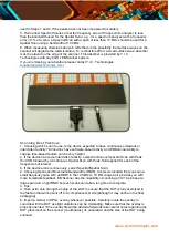
Place the PCB on the scanner aligning it as closely as possible to the vertical and horizontal
guidelines. Lining it up squarely assists you when importing overlays or images (JPG).
When analyzing the emissions produced by a printed circuit board or device (DUT), verify
that the signals are actually being emitted from the DUT and are not ambient background
signals being retransmitted by the DUT:
1. Run a Spectral Scan over the frequency range of interest with the unpowered PCB on
scanner. This is to eliminate the possibility that the DUT is acting like an antenna or signal
conduit for non-local sources.
2. Power on the PCB and go through step 1.
3. Compare the powered and unpowered scans taken with the DUT in the identical positions
and with identical scanning parameters to identify frequencies that have emissions
emanating from the DUT. To determine the significant emission areas on the DUT at the
frequencies of interest:
4. Perform a wide-frequency range Spectral/Spatial Scan or several Spectral/Spatial Scans
to cover the entire frequency range of interest. Run Spatial Scans at the same frequencies


