550 Granite Court, Pickering, Ontartio CANADA L1W-3Y8
4625 Witmer Industrial Estate, Niagara Falls, New York USA 14305
SERVICE MANUAL
2
Yorkville Sound
• http://www.yorkville.com
CIRCUIT DESCRIPTION:
The voltage amplifier is a mirrored image with circuitry connected to the positive power
supply rail being identical (but opposite polarity) to the circuitry connected to the nega-
tive power supply rail.
For this reason we will look in detail at the positive side of the amplifier.
The audio signal enters the voltage amplifier at the SIG input. The signal passes
through R40A, D14A and D13A to the base of Q12A. Diodes D13A and D14A set up
the DC bias on Q12A to approximately 0.6 mA.
The first voltage gain stage consists of Q12A along with the resistor chain on its col-
lector and the emitter resistor (R44A).
Transistor Q12A drives the base of Q14A through the resistor chain. A DC current of
approximately 4 mA should flow through the collector of Q14A. The voltage drop
across Q14A remains constant and is derived from the voltage drop across the voltage
reference Q20A, resistor R58A, and the base/emitter junction of Q15A. This total volt-
age should equal approximately 3 VDC. Transistor Q14A is the second gain stage and
its output current flows through Q15A. Transistor Q15A is a common base stage with
the collector driving the base of output buffer Q18A.
Diode D17A is a clamping diode that prevents the maximum peak of the audio sig-
nal from coming within 4V of the 144 VDC rail. This is to prevent the output current
amplifier from going into saturation during clipping and therefore having storage delay
problems.
Transistor Q18A buffers the high impedance present on the collector of Q15A. The
output of the buffer provides a low output impedance at the junction of R61A and
R62A and is current limited to 30mA through the clamping action of D19A, D20A and
D23A. The signal at the junction of R61A and R62A drives the succeeding current
amplifier.
Current Amplifier Section
The current amplifier receives a high voltage audio signal from the voltage amplifier
and provides the current drive necessary to drive speaker cabinets.
The current amplifier is a two-tier complimentary output driver design controlled by a
complimentary darlington stage.
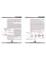
[CIRCUIT DESCRIPTION - REFER TO THE SIMPLIFIED SCHEMATIC #1 ON THE
FOLLOWING PAGE]
550 Granite Court, Pickering, Ontartio CANADA L1W-3Y8
4625 Witmer Industrial Estate, Niagara Falls, New York USA 14305
SERVICE MANUAL
Yorkville Sound
• http://www.yorkville.com
QUIESCENT CONDITION:
This design is class A/B and therefore the output driver transistors must be forward
biased to provide low crossover distortion. In most class A/B designs, a diode chain or
VBE multiplier is used to control the bias voltage and provide a means of adjusting the
bias. This design is different, as there isn’t a diode chain or VBE multiplier. For simplici-
ty lets consider only the positive side of the current amplifier, that is all parts between
the positive power supply rails and the audio signal output/input terminals. The nega-
tive side is the same as the positive, except for polarity changes.
To bias Q14, greater than 0.5V is needed from base to emitter, (or for simplicity from
base to amplifier output). Points A and B are at the same potential, so consider them
to be connected. If this is true then 0.5V from test point 2 to the amplifier output must
appear across R12. There must be some way of developing this voltage across R12,
and there is using the darington (Q5 and Q40) driver along with local feedback.
Simplified schematic #1 shows the biasing circuit. The current needed to develop 0.5V
across R12 comes from the emitter of Q5. When the amplifier is first turned on the current
source (Q3) turns on Q5 and Q40) and current flows through R12 developing a voltage.
When this voltage approaches 0.5V Q1 turns on and robs current from the base of Q40.
2


