background image

550 Granite Court, Pickering, Ontartio CANADA L1W-3Y8

4625 Witmer Industrial Estate, Niagara Falls, New York USA 14305

SERVICE MANUAL

3

Yorkville Sound

• http://www.yorkville.com

550 Granite Court, Pickering, Ontartio CANADA L1W-3Y8

4625 Witmer Industrial Estate, Niagara Falls, New York USA 14305

SERVICE MANUAL

3

Yorkville Sound

• http://www.yorkville.com

This causes Q40 to turn off until the reduced current flowing through Q5 maintains

0.5V across R12. Q1 will turn off slightly causing Q5 and Q40 to increase their collector
currents. The circuit reaches a point of equilibrium with approximately 0.5V across R12.

Because all output devices are not identical and base emitter voltages vary, some

adjustment must be available to slightly adjust the 0.5V across R12. This is accom-
plished with RT1. RT1 causes Q1 to turn on slightly more or less resulting in Q5 and
Q40 turning on slightly more or less and therefore R12’ s voltage will be slightly more
or less than 0.5v. The proper quiescent current voltage is 4mV  (to be measured
between test points 8 and 9).

The Second Tier and Tier Switching

Refer to the simplified schematic Fig. #1 while reading the following text. One way of
making an amplifier more efficient is to vary the Power Supply Voltage on the collec-
tors of the output transistors (Q14 & Q22). The lower the voltage from collector to emit-
ter, the lower the device dissipation. During quiescent conditions, there is 55VDC on
the collectors of output transistors Q14 and Q22. The peak AC voltage that can appear
on the amplifier’s output is approximately 139V peak. How can an output transistor
deliver a 139V peak when its collector is only at 78VDC? It can if its collector is pulled
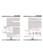
up to 144VDC as the output signal’s peak rises above 78VDC. Refer to Fig. #2. The
second tier voltage must remain above the amplifier’s output voltage by amount Vm.
Therefore the circuitry controlling the second tier voltage must increase the tier voltage
before the amplifier’s output voltage reaches 78VDC. This leading voltage is necessary
to compensate for time lag of the second tier circuit during fast rising amplifier output

signals.

The voltage between the amplifier’s output

and test point 4 is approximately 12VDC
derived from the voltage drop across ZD4. We
call this voltage the “floating battery” because it
floats on top of the output audio signal with test
point 4 always being 12VDC greater than the
peak of the output signal. Test point 4 drives the
gate of mos-fet Q11. Q11 controls the transis-
tors of the upper tier. As Q11 turns on its source
forward biases the base of Q13 and Q13 pulls
the collector of Q14 towards the 100 volt rail.
The gate to source voltage needed to turn on
Q11 is approximately 3.5 volts. When the peak
output signal is about 69.5vp (78v-(12v-3.5v))
then Q11 will start to turn on the second tier.
The second tier voltage will remain about 13
volts (Vm) above the peak of the output signal

to the point of clipping where this voltage is reduced to about 6 volts (measured dri-
ving an 8 ohm load). Zener ZD8 protects the gate source junction of Q11 and also pro-
vides a supply current path through R29 for the “floating battery”.

NOTE:

The Power supply voltages given are those when the amplifier is 

not

driving a

speaker load. This will allow yo to check the tier switching with the cover of the amplifi-
er off and the amplifier, therefore, running cool.

Current Limit Protection Circuitry

To have an amplifier drive 3000 watts into practically any combination of speaker cabi-
nets and know what is a safe load and what is not is a very difficult task. An extensive

amount of time was spent on the current limit circuitry so that it may simulate the safe
operating area of the output transistors (SOAR curve). No matter how reactive the load
may be the phase shift that it presents, along with it’s resistive component is used to
set the output current limit of the output transistor stage.

Refer to the schematic of board M1146 while reading the following text. The current
limit circuitry is a mirrored image with circuitry connected to the positive power supply
rail being identical (but opposite polarity) to the circuitry connected to the negative
power supply rail. For this reason we will look at the positive side of the circuitry.

Transistor Q9 measures the peak current flowing through resistor R53. The voltage
across R53 (as a result of the current flowing through it) is scaled down by R55, R35,
R35A, R36, R37, D7 and D11 these parts make up the safe operating area along with
the time constants of C30, R34, C12 and R26. Fig. #3 shows a waveform of the current
that passes through R52 and R53 when the output of the amplifier is shorted to ground.
This can only be seen by using an oscilloscope to measure differentially across R52
and R53. The conditions of the measurement are contained on the diagram. During cur-
rent limit when Q9 turns on it reduces the voltage across R42. R42 is in series with a
16 volt zener (ZD7) and is also in parallel with the junction of Q8. The current that flows
through R20, ZD7, R42, and R22 normally saturates Q8. When Q9 reduces the voltage
across ZD9 and R42 to below 16.6 volts, Q8 turns off allowing a charge to build up on
C8 through resistors R24 and R25. If current limiting occurs for a long enough duration
to allow C8 to charge to 1.2 volts then Q7 will turn on tripping the relay circuit on board
M1147. As soon as the relay is tripped the audio signal will be turned off at the output
of the voltage amplifiers and will remain off for about 5 seconds before the relay turns
on and allows the audio signal to pass through the amplifier. If a current limit condition
is still present then the whole cycle will occur again and repeat until the load conditions
on the amplifier’s output are safe for the amplifier. When a safe load appears the ampli-
fier will automatically reset and drive that load (the speaker cabinet).

DC Protection

If a DC voltage greater than 8 volts appears on the output of the amplifier for more
than 200 milliseconds then triac Q30 will turn on holding the output at ground poten-
tial. MBS4992 is a device that turns on at or - 8 volts DC.

Summary of Contents for Professional AP4040

Page 1: ...ra Falls New York 14305 USA Voice 716 297 2920 Fax 716 297 3689 WORLD HEADQUARTERS CANADA Yorkville Sound 550 Granite Court Pickering Ontario L1W 3Y8 CANADA Voice 905 837 8481 Fax 905 837 8746 Quality and Innovation Since 1963 Printed in Canada WEB www yorkville com MODEL TYPE YS4040 ...

Page 2: ... spilled or objects have fallen into the apparatus the apparatus has been exposed to rain or moisture does not operate normally or has been dropped AVIS AFIN DE REDUIRE LES RISQUE DE CHOC ELECTRIQUE N ENLEVEZ PAS LE COUVERT OU LE PANNEAU ARRIERE NE CONTIENT AUCUNE PIECE REPARABLE PAR L UTILISATEUR CONSULTEZ UN TECHNICIEN QUALIFIE POUR L ENTRETIENT Instructions relatives au risque de feu choc élect...

Page 3: ...1 FILTER FOAM 1 6909 MJ21196 TO3 NPN TRAN TH 16 3468 8 3 16 SJT AC LINE CORD STRIP 17 1 4771 1 4W 17K8 1 T R RES 2 6910 MJ21195 TO3 PNP TRANSISTOR TH 16 3821 STRAIN RELIEF HEYCO 1200 1 6125 1 4W 18K 5 MINI T R RES 2 7004 2SA2121 0 TO3P PNP TRAN TK 2 8261 GE VELVET MATTE LEXAN 007 X12 X24 0 348 6123 1 4W 20K0 1 MINI MF T R RES 4 7005 2SC5949 0 TO3 NPN TRANSISTOR TK 2 8701 4 40 KEPS NUT ZINC 20 4777...

Page 4: ...iting the audio signal at U2 The charging attack and discharging release times of the limiter are 80mS and 3 5 seconds respectively Resistors R50 and R7 provide the charging path and resistor R51 provides the dis charge path The limiter can be defeated by placing the limiter switch S2 in the in position which disconnects Q5 and the charging discharging circuitry from V The activity LED circuit con...

Page 5: ...ction of D19A D20A and D23A The signal at the junction of R61A and R62A drives the succeeding current amplifier Current Amplifier Section The current amplifier receives a high voltage audio signal from the voltage amplifier and provides the current drive necessary to drive speaker cabinets The current amplifier is a two tier complimentary output driver design controlled by a complimentary darlingt...

Page 6: ...uced to about 6 volts measured dri ving an 8 ohm load Zener ZD8 protects the gate source junction of Q11 and also pro vides a supply current path through R29 for the floating battery NOTE The Power supply voltages given are those when the amplifier is not driving a speaker load This will allow yo to check the tier switching with the cover of the amplifi er off and the amplifier therefore running c...

Page 7: ... occurs With the voltage amplifiers now disabled there is no signal driving the output transistors Q13 to Q28 The current limit circuit protecting the output transistors Q13 to Q28 turns off and D204 and or D205 are not forward biased and Q202 turns off Through Q203 and Q201 the relay is turned back on and the voltage amplifiers are now active again dri ving the output transistors If current limit...

Page 8: ... quiescent conditions there should only be 3 to 5 millivolts across test points 8 and 9 on the out put stage of the amplifier 5 Yorkville Sound http www yorkville com is 10 volts across R235 or R236 which is enough to turn on Q210 Q208 and Q207 pro viding 7 DC volts to the fan Further heating the temperature sensors results in a larger DC voltage across the fan To lower the dissipation of Q207 D21...

Page 9: ...te for one s lack of electronic capability Before starting look at the board for repair and locate the version number It is very important that you follow the procedure for the appropriate circuit board version number A complimentary service manual for the AP4020 power amplifier is sup plied with this M1146KIT STEP 1 Locate the assembly drawing for the version number printed on the M1146 or M1126 ...

Page 10: ... there is still a damaged part on the board instantly turn ing it on could blow up the board and you would be back where you started Connect the power wires and ground to the power supply Connect a digi tal multimeter to test pins 8 and 9 to measure the bias quiescent current and place a scope probe on the speaker output Be sure to turn the quies cent current trimpot RT1 fully counter clockwise No...

Page 11: ...unction 5908 63V C8 100N R3 1 4W MINI 470K R36 1 4W MINI 8M2 VCC LM13600N Dual VCA 6745 U3 C Function 1N5225B 3V0 D1 0W5 12 12 W1 L 10 12 W1 J 6 12 W1 F 8 12 W1 H 2 12 W1 B 4 12 W1 D B E TO 92 BC560C C BC550C W2 3604 M AUD P1 4390 10K Function R32 1 4W 15K M AUD P2 4390 10K Function R49 1 4W 15K R33 1 4W 10K R48 1 4W 10K R30 1 4W MINI 1K TO92 BC560C Q4 5102 R52 1 4W MINI 1K 1 4W 22M R65 1 4W 22M R...

Page 12: ... 78K7 14K7 100N 62K 47K 15K 249R 620R 220R 220R 1K2 470N 15K 15K 15K 47K 249R 47P 82K 14K7 4148 GRN BC560C GRN 10K BC560C 220P RED MPSA63 RED LM13600N 10K AUD 100N 10K AUD M1128 M1133 LCLP BRPRTCT LREF RREF RSIG V V LIMABLE M1128 AP VX M1133 VTC LREF RREF ACT AP VX VTC LVGND V V800 PRTCT V RSPOST LSPRE RSPRE X8011 RSIG LSPOST LSPOST RCLP R17 R8 R57 R58 X22 X19 R25 R15 C21 R28 R19 C37 R55 R59 R36 X...

Page 13: ...M1128 AP VX 2 3511 POT 1 P22 PT 3739 SCREW SPACER LED 8870 WASHER 0 4 PCB SEE LAYOUT DIAGRAM X8011 PRODUCTION NOTES ...

Page 14: ...1 DATE MODEL S VER DESCRIPTION OF CHANGE OCT 97 1 00 FIRST PRODUCTION APR 17 98 2 00 5664 RIBBON CABLE CONNECTIONS CHANGED FOR PROTECT CIRCUIT DEC 09 98 3 00 PC 5736 TRACES CHANGED POT SUPPORT SCREWS ADDED NOV 20 01 3 10 PC 6466 LD7 LD8 NSL28AA NSL32SR2 JUL 09 02 4 00 PC 6401 PARTS MOVED NEAR P2 OCT 25 02 4 10 PC 6568 R44 R41 10K 1K APR 15 05 5 00 PC 6873 REDO SOLDERMASK JUN 05 06 6 00 PC 7138 GT ...

Page 15: ... 100V S1 B FILTER SW C33 68N 100V C34 68N 100V 1 4W R23 0 1 9K76 C9 220P 100V 4148 D7 U3 A MC33078P 8 V 4 V U4 C 8 V 4 V U3 C MC33078P U4 B C13 100V 100N S T R J4 S T R J3 C15 100N 50V COM M R L MONO STEREO BRIDGED 3705 S3 D 1 4W R6 33K U4 A MC33078P 1 8W R112 10R C16 100N 50V W1 3570 U1 B MC33078P COM M R L 3705 S3 A MONO STEREO BRIDGED 13 10 7 4 1 9 11 12 8 2 3 5 6 VER MODEL S DATE DESCRIPTION O...

Page 16: ... 150N 68N 4148 56K 150N 9K76 68N MC33078P 150N 1K54 220P 100N 9K76 68N 33K 1K54 220P 14 PIN SCKT 100N 275V 22N V V LIMABLE RIGHT RSPOST RSIG LSPOST LSPRE RREF AP2020 AP4020 AP4040 RSPRE LREF M1129 LEFT V6 00 FROM POTS BRIDGED STEREO MONO R14 W4 R37 R24 C10 R18 X31 R12 X29 X26 X119 X23 R22 X43 R26 R20 R28 R10 X19 C30 X50 C5 C8 TP4 R38 X35 X10 R112 X32 C32 R109A R11 C14 C13 W3 C6 R13 X17 C15 R15 C7 ...

Page 17: ...SK M1129 Database History CONVERT TO PCAD2002 PC 6944 ROUTE GAUGE PC 6914 ADD TARGETS AUG 15 2005 4 1 6 5 3 2 MODEL S PC PLACE IMPLEMENTED CHANGES INTO BOARD HISTORY PENDING CHANGE X X X X X X PC PC PC PC PC PC M1129 PENDING CHANGES AP2020 AP4020 AP4040 AM1CE 12 9 6 3 13 11 10 5 4 8 7 2 1 DATE MODEL S VER DESCRIPTION OF CHANGE D D JUL 2005 DEC 02 97 V V 3 00 N N CONVERT TO PCAD2002 C27 C28 C29 C30...

Page 18: ...Function 2 2_ J1 B 3628 SPEAKON 4C Function 1 1_ J1 A 3628 SPEAKON 4C Function C E B R86 1 4W MINI 470R R69 1 2W 22K R64A 1 4W FUSIBLE 151R GND VCC OUT AS35FN TO 92 Watts Q31 6478 Function R42A 1 4W 56K R51A 1 4W MINI 1K5 TO92 BC550C Q17A 5101 R41A 1 4W 7K5 TO92 MPSA92 Q13A 5114 R71 1 4W MINI 100K 4148 D21A R44A 1 4W MINI 1K TO92 MPSA42 Q12A 5113 C20A 400V 2N2 4148 D19A 4148 D20A R47A 1 4W MINI 1K...

Page 19: ...K 22N 43K 200R0 47 00 U 80 V MBS4992 TO92 22K 1 2W 22K 1 2W 22K 1 2W 22K 1 2W 4 U H MR854 MR854 151R 39R0 3K3 4N35 33V0 TO220 IRF630NPBF MR854 MR854 MR854 12V0 22U 50V 470 0U 80V 4 7 0 0 U 8 0 V 4 7 0 0 U 8 0 V 470 0U 80V 5 0W 0R1 5 0W 0R1 M J 2 1 1 9 6 B o d y M J 2 1 1 9 5 B o d y MJ21195 Body 10U 63V 5 0W 3K6 47 00U 80 V MJE340 BC550C 160V 10U 5 0W 0R1 5 0W 0R1 MJ21195 Body M J 2 1 1 9 5 B o d ...

Page 20: ...TER MOUNTING DEVICE DO NOT CUT LEGS BEND LEGS IN DIRECTION SHOWN IT IS IMPRATIVE THAT LEG ARKED 2 AND 3 ARE BENT FLAT AGAINST THE COPPER SURFACE COOLED FROM WAVE SOLDER IS 6 INCH LB INITIAL TORQUE FOR TO 3 S IS 8 INCH LB 6 USE 2006 SMALL BODY 1R 1W FOR R33 AND R49 3851 1 2 PCB PLASTIC SPACER 5 MOUNTING HARDWARE FOR TO3 OUTPUTS 8701 4 40 KEPS NUT 8667 SHOULDER WASHER 2 MOUNTING HARDWARE FOR Q5 AND ...

Page 21: ...7 1W PC 5767 C10 C15 C20A 2N2 TO PT 5427 DERIVED FROM M1126 PC 5908 U1 U2 4N35 TO TLP621 SPKON JACKS RE CONFIGURED CORRECT ERROR IN SPKONS M1146 Database History AP4040 V44 N C MT1 MT2 MBS4942 12 9 6 3 13 11 10 5 4 8 7 2 1 DATE MODEL S VER DESCRIPTION OF CHANGE D D D V V V V V D D N N N N N D D D V V V AP4040 V 2 20 V V V APR 25 06 MAY 02 06 D D D M1146 SCH_DATABASE_HISTORY N N N PC 7083 MTP10N15L...

Page 22: ...2 W35 K 12 12 W35 L 4 12 W35 D 7 12 W35 G 9 12 W35 I 2 12 W35 B 2N6517 R214 1 2W 15K R213 1 2W 15K R216 1 4W MINI 1K R215 1 4W RAD 1K R202B 1 4W 16K5 C206 25V 100U R204B 1 4W MINI 10K0 C214B 100V 220P R204A 1 4W MINI 10K0 C214A 100V 220P R203A 1 4W MINI 10K0 4148 D202B 4148 D201B 4148 D201A 4148 D202A 3700 K1 B TO92 BC550C Q203 5101 R219 1 4W 7K5 R255 1 4W MINI 10K 4148 D211 TO92 MPSA06 Q208 5103 ...

Page 23: ...PC C 250V 4N7 100V 330U PRI 18 LREF LSIG ACT RSIG BRPRTCT X8012 M1134 V44 RCLIP RCLIM RDRV ROG RTSENS ROSIG ROG LCLIP LCLIM LOG LTSENS LOG LOSIG 18 12V0 RCLIP PRTCT LVGND TOP AMP M1147 M1134 RNFB RREF LCLIP TO LNFB LDRV M1147 AP4040 AP4040 V44 TO BOTTOM AMP R236 D211 TP9 R240 R244 R245 D212 D218 ZD211 X42 W9 BLK X6 X21 X8 R207 X10 C214B R218 R216 R217 ZD210 R234 ZD205 X38 X36 D215 R209 D202B X35 X...

Page 24: ...M1147 AP4040 X8012 PRODUCTION NOTES SEE LAYOUT DIAGRAM ...

Page 25: ...695 ADD TP9 10 ENLARGE AC TRACES PC 5798 REPLACE ZD212 WITH JUMPER PC 5664 ADD EXTRA PROTECT CIRCUIT REPLACE R233 THERMISTOR WITH SURGISTORS DERIVED FROM M1127 PC 6218 UPDATE REL2 SYMBOL HOLE LOCATIONS REPLACE JUMPERS FOR BRIDGE WITH TABS AND WIRES NEW SOLDERMASK FOR TABS X8012 Database History AP4040 AND V44 BC560C BC550C MJF6388 MJF6668 6 3 5 4 8 7 2 1 DATE MODEL S VER DESCRIPTION OF CHANGE D D ...

Reviews: