CLM920_TE5 LTE Module Hardware Manual
28
YUGA Information Technology Co.,Ltd
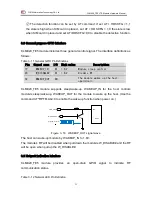
the module to the external audio power amplifier signal.
③
The audio signal is a sensitive signal, the alignment should be careful to protect
against interference, keep away from the RF interference area, connection lines as
short as possible and protect sensitive signals when layout.
④
In order to prevent noise of TDD, design of audio circuit should reserved filter
capacitance of 10 pF and 33 pF, which to remove radio frequency interference signal.
⑤
Users can set to handset output by AT+CSDVC=4, headset output by
AT+CSDVC=2. Adjust the handset output volume gain by AT+COUTGAIN and set
the Mic gain by AT+CMICGAIN. More details refer to the AT manual.
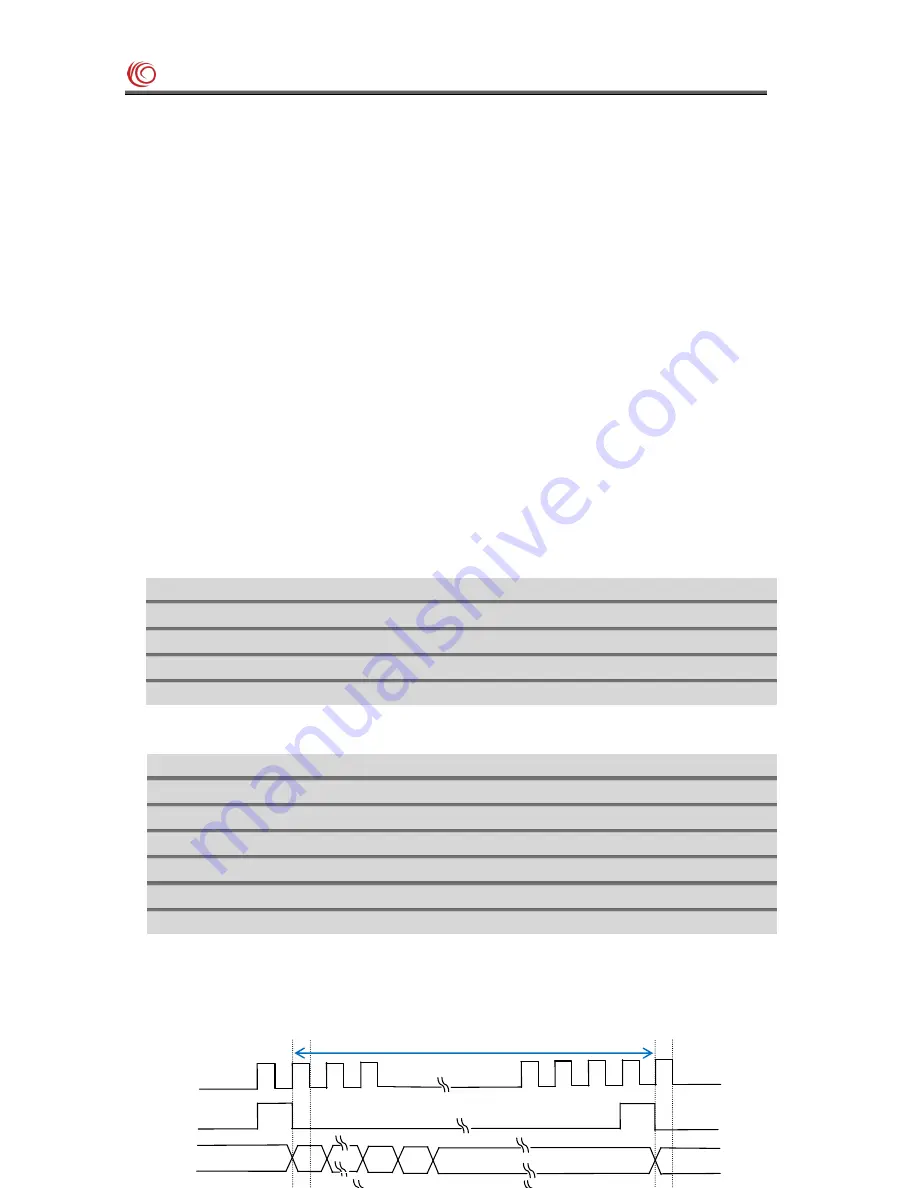
3.11 PCM audio interface
CLM920_TE5 module provides one PCM audio interface, which supports 8-bit A-law and
μ-law, 16-bit linear data formats, PCM_SYNC is 8kHZ, PCM_CLK is 2048kHZ。
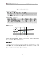
Table 3- 15 PCM Pin Definition
Pin
Signal Name
I/O
Description
45
PCM_CLK
D0
PCM clock signal
47
PCM_DOUT
D0
PCM data output
49
PCM_DIN
DI
PCM data input
51
PCM_SYNC
DO
PCM frame sync
Table 3- 16 PCM Parameter
Feature
Description
Data Format
linear
Data bit
16bits
PCM role
Master/Slave
PCM Clock
2048kHz
PCM Frame Sync
short
Transfer
MSB
256
LSB
LSB
MSB
MSB
PCM_SYNC
PCM_CLK
125us
PCM_OUT
1
2


