background image

User’s Manual

3

1.3  Optional Add-Ons

Plastic enclosure (can be wall-mounted or panel-mounted), which consists of a base 
and a cover for either the LP3500 by itself or an assembly made up of the LP3500 and 
the LP3500 Prototyping Board. The base is also available separately.

The Prototyping Board included with the Tool Kit is a convenient means of  interfacing 
to the LP3500 via the screw-terminal headers on the Prototyping Board. The Prototyp-
ing Board is also available for separate purchase.

4M and 8M serial flash expansion cards.

 LCD/keypad module with  7-key keypad and seven LEDs.

Further details on the Prototyping Board, the plastic enclosure, and the LCD/keypad mod-
ule are provided in Appendix B, Appendix C, and Appendix D.

Visit Z-World’s Web site for up-to-date information about additional add-ons and features 
as they become available. The Web site also has the latest revision of this user’s manual 
and schematics.

Summary of Contents for Fox LP3500

Page 1: ...Fox LP3500 C Programmable Single Board Computer User s Manual 019 0111 041029 E ...

Page 2: ...00 User s Manual Part Number 019 0111 041029 E Printed in U S A 2002 2004 Z World Inc All rights reserved Z World reserves the right to make changes and improvements to its products without providing notice Trademarks Rabbit and Rabbit 3000 are registered trademarks of Rabbit Semiconductor Dynamic C is a registered trademark of Z World Inc ...

Page 3: ... Subsystems 17 3 1 LP3500 Pinouts 18 3 1 1 Headers and Screw Terminals 18 3 2 Power Modes 19 3 2 1 Setting the Power Save Mode 20 3 2 2 Operating in the Power Save Mode 21 3 2 3 Resuming Normal Power or Low Power Operation 21 3 3 Digital I O 22 3 3 1 Digital Inputs 22 3 3 2 Digital Outputs 23 3 4 Serial Communication 25 3 4 1 RS 232 26 3 4 2 RS 485 26 3 4 3 Serial Interface Port 28 3 4 4 Programmi...

Page 4: ...only 64 4 5 7 PWM Outputs 65 4 6 Relay Output LP3500 only 66 Appendix A LP3500 Specifications 67 A 1 Electrical and Mechanical Characteristics 68 A 1 1 Exclusion Zone 71 A 1 2 Headers 72 A 2 Conformal Coating 73 A 3 Jumper Configurations 74 A 4 Use of Rabbit 3000 Parallel Ports 77 Appendix B Prototyping Board 81 B 1 Mechanical Dimensions and Layout 82 B 2 Using the Prototyping Board 83 B 2 1 Inter...

Page 5: ...teries and External Battery Connections 121 E 2 1 Replacing the Backup Battery 122 E 2 2 Power to VRAM Switch 122 E 2 3 Reset Generator 123 E 3 Chip Select Circuit 123 Appendix F Programming Cable 125 Appendix G Running a Sample Program 129 Notice to Users 131 Index 133 Schematics 137 ...

Page 6: ...Fox LP3500 ...

Page 7: ...MI Rabbit 3000 microprocessor flash memory static RAM digital I O ports A D converter inputs PWM outputs RS 232 RS 485 serial ports and both parallel and serial interfaces that allow other devices to be connected to the LP3500 All aspects of the LP3500 are designed for low power consumption and operates at a vari ety of power levels including a power save mode to fit customer specified conditions ...

Page 8: ...atchdog supervisor Two LP3500 models are available Their standard features are summarized in Table 1 Appendix A provides detailed specifications The LP3500 can be mounted in two ways It can be mounted to a panel or on a plastic enclosure base which allows I O connections to be made using traditional connectors with 0 1 spacing The LP3500 can also be inverted and mounted directly to mating connecto...

Page 9: ...o the LP3500 via the screw terminal headers on the Prototyping Board The Prototyp ing Board is also available for separate purchase 4M and 8M serial flash expansion cards LCD keypad module with 7 key keypad and seven LEDs Further details on the Prototyping Board the plastic enclosure and the LCD keypad mod ule are provided in Appendix B Appendix C and Appendix D Visit Z World s Web site for up to ...

Page 10: ... you to develop your own add on circuits The screw terminal headers extend the LP3500 s headers for development and can also be used in a production environment Plastic enclosure with four screws Four stand offs with mounting screws Screwdriver Rabbit 3000 Processor Easy Reference poster Registration card Figure 1 Tool KitLP3500 Tool KitTool Kit PROG DIAG Programming Cable 101 0276 Screwdriver Use...

Page 11: ... C Web based technical support is included at no extra charge Z World also offers add on Dynamic C modules containing the popular µC OS II real time operating system as well as PPP Advanced Encryption Standard AES and other select libraries In addition to the Web based technical support included at no extra charge a one year telephone based technical support module is also available for purchase V...

Page 12: ...eries of single board computers meets the following EN55024 1998 immu nity standards EN61000 4 3 Radiated Immunity EN61000 4 4 EFT EN61000 4 6 Conducted Immunity Additional shielding or filtering may be required for a heavy industrial environment Emissions The LP3500 series of single board computers meets the following emission standards emission standards with the Rabbit 3000 spectrum spreader tu...

Page 13: ...microprocessor may result if voltages outside the design range of 0 V to 40 V DC are applied directly to any of its digital inputs The lithium backup battery circuit on the LP3500 has been designed to protect the bat tery from hazardous conditions such as reverse charging and excessive current flows Do not disable the safety features of the design 1 5 2 Interfacing the LP3500 to Other Devices Ther...

Page 14: ...8 Fox LP3500 ...

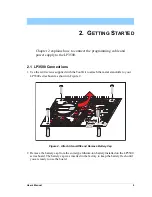
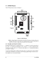
Page 15: ... R40 C54 R 3 7 C 2 4 R30 D 1 9 D 2 0 D21 D18 D25 Q 5 R 4 2 Q6 R43 R33 Q 8 Q10 D 2 6 D 2 8 Q16 D 3 0 Q17 D 3 4 K1 Q13 D32 D33 Q14 J6 C67 C55 R44 R47 U11 S1 RESET J5 J2 PROGRAM PORT AIN0 AIN1 AIN2 AIN3 AIN4 AIN5 AIN6 AIN7 GND GND VBAT EXT GND VIN GND P W M 0 P W M 1 P W M 2 GND D IS P L A Y R 5 5 R 5 6 J 9 J8 RELAY N O C O M N C C48 U3 R 5 7 R 3 1 C 2 9 R 2 3 C22 C20 C 1 2 C 1 5 D 1 5 D 1 7 R P 1 7 ...

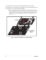
Page 16: ... OUT7 OUT6 OUT5 OUT4 OUT3 OUT2 OUT1 OUT0 GND VIN GND VBAT EXT GND PWM2 PWM1 PWM0 GND AIN7 AIN6 AIN5 AIN4 AIN3 AIN2 AIN1 AIN0 GND IN 15 IN 14 IN 13 IN 12 IN 11 IN 10 IN 09 IN 08 G N D IN 07 IN 06 IN 05 IN 04 IN 03 IN 02 IN 01 IN 00 G N D J2 J21 J22 J23 J 1 1 J 1 2 J 1 J 1 3 J41 J42 J4 J43 J44 G N D V IN LP3500 Prototyping Board S1 S2 S3 S4 RN1 D S 4 D S 3 D S 2 D S 1 D1 P W R J5 R1 V IN G N D VIN G...

Page 17: ... default COM port used by Dynamic C Figure 4 Programming Cable and Power Supply Connections GND RxE TxE GND RxC TxC GND RxB TxB GND 485 GND K OUT9 OUT8 OUT7 OUT6 OUT5 OUT4 OUT3 OUT2 OUT1 OUT0 GND VIN GND VBAT EXT GND PWM2 PWM1 PWM0 GND AIN7 AIN6 AIN5 AIN4 AIN3 AIN2 AIN1 AIN0 GND IN 15 IN 14 IN 13 IN 12 IN 11 IN 10 IN 09 IN 08 G N D IN 07 IN 06 IN 05 IN 04 IN 03 IN 02 IN 01 IN 00 G N D J2 J21 J22 J...

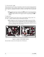
Page 18: ...D18 D25 Q5 R42 Q6 R43 R33 Q8 Q10 D26 D28 Q16 D30 Q17 D34 K1 Q13 D32 D33 Q14 J6 C67 C55 R44 R47 U11 S1 RESET J5 J2 PROGRAM PORT AIN0 AIN1 AIN2 AIN3 AIN4 AIN5 AIN6 AIN7 GND GNDVBAT EXT GND VIN GND PWM0 PWM1 PWM2 GND DISPLAY R55 R56 J9 J8 RELAY NO COM NC PROGRAM PORT TP2 RESET RESET JP1 JP2 JP3 JP4 JP5 JP6 JP8 JP11 JP7 JP10 JP9 JP12 RP1 D3 RP2 D6 D12 D10 RP4 RP3 D16 D14 Q3 Q4 D23 D24 Q7 D27 Q9 RP10 D...

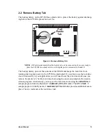
Page 19: ...r application you will need to set the real time clock once you remove the plastic tab Set the real time clock using the onscreen prompts in the demon stration program Alternatively you may set the real time clock using the SETRTCKB C sample program from the Dynamic C SAMPLES RTCLOCK folder The RTC_TEST C sample program in the Dynamic C SAMPLES RTCLOCK folder provides additional exam ples of how t...

Page 20: ... a power source start Dynamic C by dou ble clicking on the Dynamic C icon or by double clicking on the exe file associated with DcRab in the Dynamic C directory Dynamic C assumes by default that you are using serial port COM1 on your PC If you are using COM1 then Dynamic C should detect the LP3500 and go through a sequence of steps to cold boot the LP3500 and to compile the BIOS If the error messa...

Page 21: ...sed your LP3500 through a distributor or Z World partner contact the distributor or Z World partner first for technical support If there are any problems at this point Check the Z World Technical Bulletin Board at www zworld com support bb Use the Technical Support e mail form at www zworld com support If the sample program ran fine you are now ready to go on to explore other LP3500 fea tures and ...

Page 22: ...16 Fox LP3500 ...

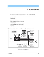
Page 23: ...y PWM Outputs Relay Output Circuit LP3500 only Memory Figure 7 shows these Rabbit based subsystems designed into the LP3500 Figure 7 LP3500 Subsystems SRAM Flash 3 7 MHz osc 32 kHz osc LP3500 Decoder Control Interface to LCD Keypad Module RABBIT 3000 RS 232 RS 485 A D Converter PWM Outputs Digital Outputs Relay Output Programming Port Serial Interface Digital Inputs ...

Page 24: ...0 1 pitch can be used to interface to the signals on headers J1 J2 and J4 or the Prototyping Board may be used to access these signals via screw terminal headers S1 RESET PROGRAM PORT GND DISPLAY J8 RELAY NO COM NC J2 GND RxE TxE GND RxC CTS TxC RTS GND RxB TxB GND RS 485 RS 485 GND K OUT9 OUT8 OUT7 OUT6 OUT5 OUT4 OUT3 OUT2 OUT1 OUT0 GND 25 24 23 22 21 20 19 18 17 16 15 14 13 12 11 10 9 8 7 6 5 4 ...

Page 25: ...stems from Table 3 Typical Current Consumption 1 Normal Modes 7 3728 MHz Normal None VIN Yes Yes 16 mA 5 mA 2 3 6864 MHz 3 1 8423 MHz 4 1 2288 MHz None 5 0 9216 MHz 6 Low Power Modes 32 768 kHz 1 0 mA 140 µA 7 16 384 kHz 8 8 192 kHz 9 4 096 kHz 10 2 048 kHz Power Save Mode 2 048 kHz See Section 3 2 1 and Section 3 2 2 VIN or external battery No No 140 µA External battery with linear regu lator tur...

Page 26: ...of three different software calls serCommAlert timedAlert or digInAlert depending on whether you wish to use Serial Port E a simple timeout or a digital input to trigger the LP3500 to resume operation in one of the other power modes If you call serCommAlert then any activity on Serial Port E will trigger the LP3500 out of the low power mode If you call timedAlert then the LP3500 is triggered out o...

Page 27: ...ld trigger a system reset and turn off the processor 3 2 3 Resuming Normal Power or Low Power Operation As long as VIN is still connected and the linear regulator has not been turned off the LP3500 will return automatically to the previous power mode once the non zero timeout specified in serCommAlert timedAlert or digInAlert has elapsed NOTE The processor will turn off if VIN is not available at ...

Page 28: ...t The digital inputs are each fully protected over a range of 0 V to 36 V and can handle short spikes of 40 V The actual switching threshold is approximately 1 40 V Anything below this value is a logic 0 and anything above is a logic 1 Pulling the digital inputs to Vcc will in crease the current consumption by about 300 µA for each digital input 330 nF 100 kW 22 kW Factory Default K GND Vcc 0 W Ra...

Page 29: ...0 mA at 36 V Figure 11 shows a wiring diagram for using the digital outputs in a sinking or a souring configuration Figure 11 LP3500 Digital Outputs TIP Turn the outputs off high for sourcing outputs and low for sinking outputs to reduce current consumption Vcc K SINKING OUTPUTS OUT0 OUT7 SOURCING OUTPUTS OUT8 OUT9 K 1 MW Current Flow Current Flow ...

Page 30: ... you are using the Prototyping Board with the LP3500 and you are using separate power sup plies for VIN and K When the LP3500 is used alone remember to connect a power supply to K pin 12 on header J7 Your K supply may be up to 36 V DC and should be capable of delivering up to 2 0 A NOTE If K is not connected the digital inputs may float which may increase your cur rent consumption Figure 12 Locati...

Page 31: ...t A the programming port can be operated alternately in the clocked serial mode In this mode a clock line syn chronously clocks the data in or out Either of the two communicating devices can supply the clock The LP3500 uses a 3 6864 MHz crystal which is doubled to 7 3728 MHz At this frequency the LP3500 supports standard asynchronous baud rates up to a maximum of 921 600 bps Table 5 lists the use ...

Page 32: ...ffectively at the LP3500 s maximum baud rate for distances of up to 15 m Logic level signals are also possible on Serial Ports B C and E by changing the 0 Ω surface mounted resistor jumper settings at locations JP1 JP6 Serial Port E can be set to listen and wake up the LP3500 when the unit is in a low power mode 3 4 2 RS 485 The LP3500 has one RS 485 serial channel which is connected to Serial Por...

Page 33: ...ND J4 J1 OUT9 OUT8 OUT7 OUT6 OUT5 OUT4 OUT3 OUT2 OUT0 OUT1 IN00 IN01 IN02 IN03 IN04 IN05 IN06 IN07 GND IN08 IN09 IN10 IN11 IN12 IN13 IN14 IN15 S1 RESET J5 J2 PROGRAM PORT AIN0 AIN1 AIN2 AIN3 AIN4 AIN5 AIN6 AIN7 GND GND VBAT EXT GND VIN GND PWM0 PWM1 PWM2 GND DISPLAY J8 RELAY NO COM NC AIN0 AIN1 AIN2 AIN3 J3 R1 Battery GND K GND 485 GND TxB RxB GND TxC RxC GND TxE RxE GND J4 J1 OUT9 OUT8 OUT7 OUT6 ...

Page 34: ...500 will down load a program from the port and then execute the program The programming port trans mits information to and from a PC while a program is being debugged The Rabbit 3000 startup mode pins SMODE0 SMODE1 are presented to the program ming port so that an externally connected device can force the LP3500 to start up in an external bootstrap mode The LP3500 can be reset from the programming...

Page 35: ...pad module which offers an operator interface with seven keys and a 122 32 graphic display Figure 15 provides the pinout for the Serial Interface Port Appendix C LCD Keypad Module provides further information on the LCD keypad module Figure 15 Display Interface Header J9 Pinout J9 BFD6 BFD4 BFD2 BFD0 BFA1 BFA3 GND LED6 LED4 LED2 LED0 DPRST VDISP BFD7 BFD5 BFD3 BFD1 BFA0 BFA2 GND GND LED5 LED3 LED1...

Page 36: ...sed over several software scaled voltage ranges The A D converter chip has an internal amplifier that works with the resistor divider net work on the analog inputs as shown in Figure 16 Figure 16 Buffered A D Converter Inputs The A D converter chip can be programmed in software to operate over the voltage ranges shown in Table 6 Table 6 A D Converter Input Ranges Gain Code Multiplier Voltage Range...

Page 37: ...he calibration constants are stored in flash memory You may calibrate the A D converter inputs at a later time using the software functions described in Section 4 5 5 A D Converter Inputs NOTE If you are using a fixed voltage range you should recalibrate your LP3500 at that range AIN7 can be used to monitor Vcc using the VccMonitorInit function While Vcc can be monitored in all the power modes Vcc...

Page 38: ...utputs The D A conversion outputs are pulse width modulated and scaled to provide an output from 0 V to Vcc approx 2 8 V Figure 17 shows the PWM outputs Figure 17 PWM Outputs PWM0 GND 1 kW PWM1 1 nF Rabbit 3000 Microprocessor ...

Page 39: ...the nor mal power modes NOTE The relay does not reset automatically when power is removed from the LP3500 Figure 18 Relay Output Circuit NOTE Switching the relay may consume up to 120 mA during the roughly 10 ms that it takes for the relay to switch Make sure that your power supply has sufficient capacity to handle this surge current to avoid putting the LP3500 into the power save mode The relay d...

Page 40: ...r size of the flash memory since it may be necessary to change the sector size in the future A Flash Memory Bank Select jumper configuration option based on 0 Ω surface mounted resistors exists at header JP10 This option used in conjunction with some configuration macros allows Dynamic C to compile two different co resident programs for the upper and lower halves of the 256K flash in such a way th...

Page 41: ...nnected All standalone applications can only run from flash memory The disadvantage of using flash memory for debug is that interrupts must be disabled for approximately 5 ms whenever a break point is set in the program This can crash fast inter rupt routines that are running while you stop at a break point or single step the program Flash memory or RAM is selected on the Options Project Options C...

Page 42: ...tory containing the patch Do not simply copy over an entire file since you may overwrite a bug fix of course you may copy over any programs you have written Once you are sure the new patch works entirely to your satisfaction you may retire the existing installation but keep it available to handle legacy applications 4 1 2 Upgrades Dynamic C installations are designed for use with the board they ar...

Page 43: ...2 R26 R29 C37 R32 C40 Y1 D22 C50 R36 R40 C54 R37 C24 R30 D19 D20 D21 D18 D25 Q5 R42 Q6 R43 R33 Q8 Q10 D26 D28 Q16 D30 Q17 D34 K1 Q13 D32 D33 Q14 J6 C67 C55 R44 R47 U11 S1 RESET J5 J2 PROGRAM PORT AIN0 AIN1 AIN2 AIN3 AIN4 AIN5 AIN6 AIN7 GND GNDVBAT EXT GND VIN GND PWM0 PWM1 PWM2 GND DISPLAY R55 R56 J9 J8 RELAY NO COM NC C48 U3 R57 R31 C29 R23 C22 C20 C12 C15 D15 D17 RP17 D13 BT1 D11 D5 D7 D2 D4 C8 ...

Page 44: ... SAMPLES LP3500 POWER C This program demonstrates switching from the normal raw DC power source to an external battery using the Prototyping Board Pressing a switch will change from the power source and will be displayed by flashing LEDs LOWPWRDEMO C This program demonstrates a low power mode with the normal power source connected to the LP3500 4 3 2 Digital I O The following sample programs are f...

Page 45: ...nverter channel Coefficients are read from the A D con verter s simulated EEPROM in flash memory to compute the equivalent voltages Com puted raw data and equivalent voltages are displayed in the STDIO window AD_RDVOLT_CH C This program reads and displays the voltage and equivalent values of one single ended A D converter channel Coefficients are read from the A D con verter s simulated EEPROM in ...

Page 46: ...are found in the ADC subdirectory in SAMPLES LP3500 ADCAL_ALL C This program demonstrates how to recalibrate all single ended A D converter channels using two known voltages to generate constants for each channel and will be written into the user block data area The program uses the STDIO window to display the voltage that is being monitored NOTE This sample program will overwrite the calibration ...

Page 47: ... to generate two coefficients gain and offset which are rewritten into the user block data area The program uses the STDIO window to display the current that is being moni tored NOTE This sample program will overwrite the calibration constants set at the factory 4 3 9 LCD Keypad Module Sample Programs Sample programs for the LCD keypad module are described in Section C 8 ...

Page 48: ... to the LP3500 The functions in the LP35xx LIB library are described in Section 4 5 LP3500 Function APIs Two other library directories provide libraries of function calls that are used to develop applications for the optional LCD keypad module DISPLAYS GRAPHIC libraries associated with LCD display KEYPADS libraries associated with the keypad The LCD keypad module functions are described in Section...

Page 49: ...ES all devices state 0 shuts or powers down listed devices 1 activates listed devices Table E 1 provides further information about the power consumption associated with each section RETURN VALUE 0 if valid parameter 1 otherwise SEE ALSO powerMode anaInConfig brdInit int devPowerSet int devices int state Macro Description state 0 state after Board Initialization RS232DEV Receivers and transmitters ...

Page 50: ... software defined modes RETURN VALUE 0 if valid parameter 1 if invalid parameter SEE ALSO devPowerSet rdPowerState setPowerState VccMonitor int powerMode int mode Mode Description Typical Current Consumption Debug Capable 1 CCLK PCLK MainOsc 7 3728 MHz 5 16 mA Yes 2 CCLK PCLK MainOsc 2 3 6864 MHz 3 CCLK PCLK MainOsc 4 1 8423 MHz 4 CCLK PCLK MainOsc 6 1 2288 MHz No 5 CCLK PCLK MainOsc 8 0 9216 MHz ...

Page 51: ... the real time clock until a timeout occurs The function call forces the LP3500 to enter the low power mode disables the normal power source and may enable the external battery for polling Upon expiration of the timeout this function will enable the normal power mode and exit If the normal power source is not available the LP3500 will not be able to rsume operation at the maximum power mode and ma...

Page 52: ... maxpowermode is the maximum operating power mode setting to enter usually 1 see power Mode powersource 1 battery 2 raw DC power timeout is the timeout in seconds if an input is not received Enter 0 for no timeout SEE ALSO powerMode serCommAlert timedAlert devPowerSet Determines if the LP3500 is running under battery power or a raw DC power source RETURN VALUE 0 if on raw DC power source 1 if on b...

Page 53: ...as successful Summary of Initialization LP3500 uses main oscillator LCD keypad module buffer is disabled RS 485 serial communication is not enabled RS 232 serial communication is enabled Unused configureable inputs are tied and unused configureable outputs are set low Self timed chip select is set to 109 ns If A D converter chip is installed chip is reset and SCLKD is set to 19 200 bps If A D conv...

Page 54: ...digBankOut Writes the state of a block of designated digital output channels The first bank consists of OUT0 OUT7 the second bank consists of OUT8 OUT9 A run time error will occur for the following conditions 1 channel or value out of range 2 brdInit was not executed before executing digOut PARAMETER bank is 0 for OUT0 OUT7 1 for OUT8 OUT9 value is an 8 bit output value where each bit corresponds ...

Page 55: ...kIn Reads the state of a block of designated digital input channels The first bank consists of IN0 IN07 the second bank consists of IN08 IN15 A run time error will occur for the following conditions 1 bank out of range 2 brdInit was not executed before executing digIn PARAMETER bank is 0 for IN00 IN07 1 for IN08 IN15 RETURN VALUE An input value in the lower byte where each bit corresponds to one c...

Page 56: ...s Manual and Technical Note TN213 Rabbit 2000 Serial Port Software Use the following function calls with the LP3500 User interface to set up LP3500 serial communication lines Call this function after serXOpen Whether you are opening one or multiple serial ports this function must be executed after executing the last serXOpen function AND before you start using any of the serial ports This function...

Page 57: ...mitted is detected in the receive data buffer Block data mode disable the transmitter after the same number of bytes transmitted is detected in the receive data buffer serMode must be executed before running this function SEE ALSO serMode ser485Rx Disables the RS 485 transmitter This puts the LP3500 in listen mode which allows it to receive data from the RS 485 interface serMode must be executed b...

Page 58: ...N7 Input AIN7 RESET Input Board reset device RISE FALL Input Tied up for SCLK active on rising edge PIO_0 Input Pulled down unless driven by serial interface connection PIO_1 Input Pulled down unless driven by serial interface connection PIO_2 Input Pulled down unless driven by serial interface connection PIO_3 Input Pulled up unless driven by Vcc monitor CONVERT Input Pulled down not used BUSY Ou...

Page 59: ...he registers addressed by the instruction byte Enter 0 if per forming a read operation i anaInConfig 0x07 0x3a 0 write ref osc reg and enable baud is the serial clock transfer rate of 9600 to 57 600 bps baud must be set on the first call to this function Enter 0 in this parameter thereafter anaInConfig 0x00 0x00 9600 resets device and sets baud RETURN VALUE 0 on write operations data value on read...

Page 60: ...tables below to determine cmd cmd 0x80 gain_code 16 channel_code len the output bit length is always 12 bits unsigned int anaInDriver unsigned int cmd unsigned int len Gain Code Multiplier Voltage Range 0 1 0 20 V 1 2 0 10 V 2 4 0 5 V 3 5 0 4 V 4 8 0 2 5 V 5 10 0 2 V 6 16 0 1 25 V 7 20 0 1 V Channel Code Differential Input Lines Channel Code Single Ended Input Lines Negative input is ground 4 20 m...

Page 61: ...User s Manual 55 RETURN VALUE A value corresponding to the voltage on the analog input channel which will be 0 2047 for 11 bit A D conversions bit 12 for sign 1 for overflow SEE ALSO anaInConfig anaIn ...

Page 62: ...n code of 0 to 7 RETURN VALUE A value corresponding to the voltage on the analog input channel which will be 0 2047 for 11 bit A D conversions signed 12th bit ADOVERFLOW defined macro 4096 if overflow or out of range SEE ALSO anaIn anaInConfig anaInDriver int anaIn unsigned int channel int opmode int gaincode channel SINGLE DIFF mAMP 0 AIN0 AIN0 AIN1 AIN0 1 AIN1 AIN1 2 AIN2 AIN2 AIN3 AIN2 3 AIN3 A...

Page 63: ...te calibrations and a user gain code to set voltage range defaults to the calculation gain code NOTE Vcc monitoring is disabled when anaInCalib is running PARAMETERS channel is the analog input channel number 0 to 7 corresponding to AIN0 AIN7 opmode is the mode of operation SINGLE single ended input line DIFF differential input line mAMP milliamp input line int anaInCalib int channel int opmode in...

Page 64: ... is the second A D converter channel value 0 2047 volts2 is the voltage or current corresponding to the first A D converter channel value 0 to 10 V or 4 to 20 mA RETURN VALUE 0 if successful 1 if not able to make calibration constants SEE ALSO anaIn anaInVolts anaInmAmps anaInDiff anaInSetRange anaInVoltXGain anaInCalib brdInit Gain Code Voltage Range 0 0 20 V 1 0 10 V 2 0 5 V 3 0 4 V 4 0 2 5 V 5 ...

Page 65: ...tage value corresponding to the voltage on the analog input channel ADOVERFLOW defined macro 4096 if overflow or out of range SEE ALSO anaInCalib anaIn anaInmAmps brdInit float anaInVolts unsigned int channel unsigned int gaincode Channel Code Single Ended Input Lines Negative input is ground 0 AIN0 1 AIN1 2 AIN2 3 AIN3 4 AIN4 5 AIN5 6 AIN6 7 AIN7 Gain Code Voltage Range 0 0 20 V 1 0 10 V 2 0 5 V ...

Page 66: ...ER channel is 0 3 RETURN VALUE A current value between 4 00 and 20 00 mA corresponding to the current on the analog input channel ADOVERFLOW defined macro 4096 if overflow or out of range SEE ALSO anaInCalib anaIn anaInVolts int anaInmAmps unsigned int channel Channel 4 20 mA Input Lines Negative input is ground 0 AIN0 1 AIN1 2 AIN2 3 AIN3 ...

Page 67: ...o 7 RETURN VALUE A voltage value corresponding to the voltage on the analog input channel ADOVERFLOW defined macro 4096 if overflow or out of range SEE ALSO anaInCalib anaIn anaInmAmps brdInit float anaInDiff unsigned int channel unsigned int gaincode Channel Differential Input Lines 0 AIN0 AIN1 2 AIN2 AIN3 4 AIN4 AIN5 6 AIN6 AIN7 Gain Code Voltage Range 0 0 20 V 1 0 10 V 2 0 5 V 3 0 4 V 4 0 2 5 V...

Page 68: ...gle ended input line DIFF differential input line mAMP milliamp input line gaincode is the gain code of 0 to 7 The gaincode parameter is ignored when channel is ALLCHAN RETURN VALUE 0 if successful 1 if address is invalid or out of range SEE ALSO anaInEEWr anaInCalib int anaInEERd unsigned int channel int opmode unsigned int gaincode channel SINGLE DIFF mAMP 0 AIN0 AIN0 AIN1 AIN0 1 AIN1 AIN1 2 AIN...

Page 69: ...ingle ended input line DIFF differential input line mAMP milliamp input line gaincode is the gain code of 0 to 7 The gaincode parameter is ignored when channel is ALLCHAN RETURN VALUE 0 if successful 1 if address is invalid or out of range SEE ALSO anaInEEWr anaInCalib int anaInEEWr unsigned int channel int opmode unsigned int gaincode channel SINGLE DIFF mAMP 0 AIN0 AIN0 AIN1 AIN0 1 AIN1 AIN1 2 A...

Page 70: ...METER state 1 enable Vcc monitor 0 disable Vcc monitor SEE ALSO VccMonitor anaInConfig brdInit If Vcc monitoring is enabled the Vcc level is read by the ADS7870 A D converter and is converted to a voltage value RETURN VALUE A voltage value corresponding to the voltage on the analog input channel SEE ALSO VccMonitorInit anaInVolts brdInit void VccMonitorInit int state float VccMonitor void ...

Page 71: ... RETURN VALUE Actual frequency set This will be the closest possible match to the requested frequency SEE ALSO pwmOut Sets a voltage 0 to VDD on an analog output channel according to the percent duty cycle of the 1024 clock count cycle PARAMETERS channel is the output channel to write to 0 3 dutycycle is the percent duty or on cycle value of the 1024 clock count cycle i e 0 25 RETURN VALUE 0 if su...

Page 72: ...o to the normally closed NC RESET contact PARAMETERS relay 0 the one relay value is a value used to connect the relay common contact 0 relay normally closed NC or RESET Parallel Port PG5 1 relay normally open NO or SET Parallel Port PG4 RETURN VALUE 0 if successful 1 if the normal power source is not available int relayOut int relay int value ...

Page 73: ...User s Manual 67 APPENDIX A LP3500 SPECIFICATIONS Appendix A provides the specifications for the LP3500 and describes the conformal coating ...

Page 74: ...T EXT GND VIN GND PWM0 PWM1 PWM2 GND DISPLAY R55 R56 J9 J8 RELAY NO COM NC C48 U3 R57 R31 C29 R23 C22 C20 C12 C15 D15 D17 RP17 D13 BT1 D11 D5 D7 D2 D4 C8 C6 D8 D1 AIN0 AIN1 AIN2 AIN3 J3 R1 C3 C2 R6 R7 R9 Q22 RN1 RN2 Battery R54 RP14 RP13 Q20 U13 C64 R50 R49 Y2 C61 Q12 R45 R34 U8 C51 R39 R41 C53 R38 R48 C66 U12 U10 GND K GND 485 GND TxB RxB GND TxC RxC GND TxE RxE GND J4 J1 OUT9 OUT8 OUT7 OUT6 OUT5...

Page 75: ...122 32 graphic display Digital Inputs 16 fully protected 0 36 V DC can handle short spikes 40 V Digital Outputs 10 8 sink up to 200 mA each 36 V DC max 2 source up to 200 mA each 36 V DC max Relay Output 1 C form 1 A 30 V DC None Analog Inputs Eight single ended or four differential inputs 1 MΩ input impedance Sampling rate up to 200 samples s Eight software controlled ranges from 0 1 V to 0 20 V ...

Page 76: ... one 10 bit timer with 2 match registers Watchdog Supervisor Yes Pulse Width Modulators 10 bit free running counter and four pulse width registers Power 3 V to 30 V DC 20 mA max 7 4 MHz 100 µA max 2 kHz with linear regulator turned off Operating Temperature 40 C to 70 C Humidity 5 to 95 noncondensing Connectors 0 1 headers I O and misc signals one 1 25 two 1 17 headers Display one 2 13 header 2 mm...

Page 77: ...allow for sufficient air flow and will help to minimize any electrical or electromagnetic interference between adjacent boards An exclusion zone of 0 12 3 mm is recommended below the LP3500 Figure A 2 shows this exclusion zone Figure A 2 LP3500 Exclusion Zone When using the LP3500 with the Prototyping Board do not install any components in the prototyping area on the Prototyping Board between the ...

Page 78: ...5 header with a 2 mm pin spacing Figure A 3 shows the LP3500 footprint These values are relative to the mounting hole Figure A 3 User Board Footprint for LP3500 PROGRAM PORT 0 200 5 1 0 240 6 1 0 360 9 1 0 320 8 1 0 100 2 54 0 390 9 9 J2 J6 J9 J8 J4 J1 2 200 55 9 3 040 77 2 2 640 67 1 0 040 1 0 1 820 46 2 1 800 45 7 0 787 20 0 0 590 15 0 J5 ...

Page 79: ...echnical Note 303 Con formal Coatings C44 C43 C59 C60 U9 R16 R13 C10 C13 R17 R18 C16 C19 C36 U1 C70 R51 R58 C65 C26 C33 R20 R25 R22 R26 R29 C37 R32 C40 Y1 D22 C50 R36 R40 C54 R37 C24 R30 D19 D20 D21 D18 D25 Q5 R42 Q6 R43 R33 Q8 Q10 D26 D28 Q16 D30 Q17 D34 K1 Q13 D32 D33 Q14 J6 C67 C55 R44 R47 U11 S1 RESET J5 J2 PROGRAM PORT AIN0 AIN1 AIN2 AIN3 AIN4 AIN5 AIN6 AIN7 GND GNDVBAT EXT GND VIN GND PWM0 P...

Page 80: ...RT U2 JP12 JP8 JP11 JP7 JP10 JP9 JP1 JP2 JP3 JP4 JP6 JP5 Bottom Side J3 Top Side AIN3 AIN2 AIN1 AIN0 4 20 mA JP13 IN00 IN01 IN02 IN03 IN04 IN05 IN06 IN07 GND IN08 IN09 IN10 IN11 IN12 IN13 IN14 IN15 GND VIN GND GND PWM2 PWM1 PWM0 GND AIN7 AIN6 AIN5 AIN4 AIN3 AIN2 AIN1 AIN0 VBAT EXT OUT0 OUT1 OUT2 OUT3 OUT4 OUT5 OUT6 OUT7 OUT8 OUT9 GND GND K GND RxE TxE GND RxC TxC GND RxB TxB GND 485 CTS RTS U6 U7 ...

Page 81: ...2 Level 2 3 Logic Level JP2 TxE RS 232 Logic Level Select 1 2 RS 232 Level 2 3 Logic Level JP3 RxC RS 232 Logic Level Select 1 2 RS 232 Level 2 3 Logic Level JP4 TxC RS 232 Logic Level Select 1 2 RS 232 Level 2 3 Logic Level JP5 RxB RS 232 Logic Level Select 1 2 RS 232 Level 2 3 Logic Level JP6 TxB RS 232 Logic Level Select 1 2 RS 232 Level 2 3 Logic Level JP7 SRAM Size 1 2 128K LP3510 2 3 512K LP...

Page 82: ...ons except those across JP11 and JP12 are made using 0 Ω surface mounted resistors 390 Ω current limiting resistors are used on JP11 and JP12 JP11 Manufacturing Use 1 2 JP12 Manufacturing Use 1 2 JP13 Manufacturing Use 1 2 Table A 2 LP3500 Jumper Configurations continued Header Description Pins Connected Factory Default ...

Page 83: ...Pulled up PA7 Input IN15 Pulled up PB0 Input Power Input Detect Low when external power source is connected high for battery PB1 Input CLKA Pulled up when not driven by programming port PB2 Input IN04 Pulled up RABBIT 3000 Port A Port B Port D Port E PA0 PA7 PB0 PB5 PE0 PE1 PE4 PE5 PD0 PD7 RESET IOWR STATUS SMODE0 SMODE1 Watchdog 11 Timers Clock Doubler Slave Port Real Time Clock RAM Backup Batter...

Page 84: ...rogramming Port Serial Port A Inactive high PC7 Input RxA Programming Port Inactive high PD0 Output OUT0 Inactive low PD1 Output OUT1 Inactive low PD2 Output OUT2 Inactive low PD3 Output OUT3 Inactive low PD4 Output OUT4 Inactive low PD5 Output OUT5 Inactive low PD6 Output OUT6 Inactive low PD7 Output OUT7 Inactive low PE0 Input IN00 Pulled up PE1 Input IN01 Pulled up PE2 Output OUT8 Inactive low ...

Page 85: ...ow when external power source is connected high for battery PG0 Output RS 485 Transmit Enable Inactive low PG1 Output RS 232 Shutdown Control Inactive high PG2 Output TxF RS 485 Serial Port F Inactive high PG3 Input RxF RS 485 Inactive high PG4 Output Relay Set Inactive low PG5 Output Relay Reset Inactive low PG6 Output TxE RS 232 Serial Port E Inactive high PG7 Input RxE RS 232 Inactive high Tabl...

Page 86: ...80 Fox LP3500 ...

Page 87: ...Board included with the LP3500 Tool Kit and explains the use of the Prototyping Board to demonstrate the LP3500 and to build prototypes of your own circuits The screw terminal headers on the Prototyping Board facilitate access to the LP3500 connector pins and the Prototyping Board is available for purchase separately ...

Page 88: ... 0 45 87 mm 105 mm 11 mm Operating Temperature 40 C to 70 C Humidity 5 to 95 noncondensing Prototyping Area 2 2 3 4 56 mm 86 mm throughhole 0 1 spacing GND RxE TxE GND RxC TxC GND RxB TxB GND 485 GND K OUT9 OUT8 OUT7 OUT6 OUT5 OUT4 OUT3 OUT2 OUT1 OUT0 GND VIN GND VBAT EXT GND PWM2 PWM1 PWM0 GND AIN7 AIN6 AIN5 AIN4 AIN3 AIN2 AIN1 AIN0 GND J2 J21 J22 J23 J11 J12 J1 J13 J41 J42 J4 J43 J44 GND VIN IN1...

Page 89: ...gnals to be available GND VIN GND VBAT EXT GND PWM2 PWM1 PWM0 GND AIN7 AIN6 AIN5 AIN4 AIN3 AIN2 AIN1 AIN0 GND IN15 IN14 IN13 IN12 IN11 IN10 IN09 IN08 IN07 IN06 IN05 IN04 IN03 IN02 IN01 IN00 J11 J12 J1 J2 J4 J6 J41 J42 J43 J44 J21 J23 External Battery Connection Raw DC Power Input Pushbutton Switches S1 S2 S3 S4 DS4 DS3 DS2 DS1 D1 PWR R1 J3 3 V VBAT RS 232 PWM Outputs IN00 IN01 IN02 IN03 IN04 IN05 ...

Page 90: ... to PE0 PE1 PE4 and PE5 to demonstrate the interface to the Rabbit 3000 microprocessor NOTE Before running sample programs based on the LP3500 you will have to plug in the LP3500 to the Prototyping Board as described in Chapter 2 Getting Started B 2 3 Prototyping Area Small to medium circuits can be prototyped using point to point wiring with 20 to 30 AWG wire on the prototyping area Raw DC input ...

Page 91: ...for use with the LP3500 They are shown in Figure C 1 Figure C 1 LCD Keypad Modules Models LCD keypad modules sold prior to the launch of the LP3500 might not be voltage compatible with the LP3500 Contact your Z World sales representative or your authorized Z World distributor for further assistance in purchasing an LCD keypad module Mounting hardware and a 127 mm 5 or 60 cm 24 extension cable are ...

Page 92: ...oard Size 2 60 3 00 0 75 66 mm 76 mm 19 mm Bezel Size 4 50 3 60 0 30 114 mm 91 mm 7 6 mm Temperature Operating Range 0 C to 50 C Storage Range 40 C to 85 C Humidity 5 to 95 noncondensing Power Consumption 1 5 W maximum with backlight on The backlight adds approximately 650 mW to the power consumption Connections Connects to header J9 Display Interface on LP3500 LCD Panel Size 122 32 graphic displa...

Page 93: ... do not have a header at J5 or a contrast adjust ment potentiometer at R2 are limited to operate only at 5 V and will not work with the LP3500 The older LCD keypad modules are no longer being sold C2 R2 R1 C3 D2 C1 D1 C5 U2 JP1 R3 U1 C4 C10 CR1 R6 C13 C12 R7 R8 R25 R26 R11 R13 R14 R10 R9 R12 R15 R18 Q8 R16 Q5 R21 Q2 U5 J2 DISPLAY BOARD J4 KP1 R17 Q4 R22 Q6 R23 Q7 R20 Q3 R19 U7 C14 R24 C15 C16 U6 U...

Page 94: ... C 4 Keypad Template To replace the keypad legend remove the old legend and insert your new legend prepared according to the template in Figure C 4 The keypad legend is located under the blue key pad matte and is accessible from the left only as shown in Figure C 5 Figure C 5 Removing and Inserting Keypad Label 1 10 28 2 35 60 Keypad label is located under the blue keypad matte ...

Page 95: ...e or in hardware C 4 1 I O Address Assignments The LCD and keypad on the LCD keypad module are addressed by the CS strobe as explained in Table C 2 Table C 2 LCD Keypad Module Address Assignment Address Function 0xE000 Device select base address CS 0xExx0 0xExx7 LCD control 0xExx8 LED enable 0xExx9 Not used 0xExxA 7 key keypad 0xExxB bits 0 6 7 LED driver 0xExxB bit 7 LCD backlight on off 0xExxC E...

Page 96: ...n 1 Cut mounting holes in the mounting panel in accordance with the recommended dimen sions in Figure C 7 then use the bezel faceplate to mount the LCD keypad module onto the panel Figure C 7 Recommended Cutout Dimensions 2 Carefully drop in the LCD keypad module with the bezel and gasket attached 3 400 86 4 3 100 78 8 2 870 72 9 0 230 5 8 0 125 D 4x 3 CUTOUT 0 130 3 3 ...

Page 97: ... gasket is compressed and the plastic bezel face plate is touching the panel Do not tighten each screw fully before moving on to the next screw Apply only one or two turns to each screw in sequence until all are tightened manually as far as they can be so that the gasket is compressed and the plastic bezel faceplate is touching the panel Bezel Gasket DISPLAY BOARD U1 U2 C1 C2 C3 C4 U3 R17 J1 Q1 D1...

Page 98: ...N1 J2 C8 C7 KP1 J5 R25 R26 C44 C43 C59 C60 U9 R16 R13 C10 C13 R17 R18 C16 C19 C36 U1 C70 R51 R58 C65 C26 C33 R20 R25 R22 R26 R29 C37 R32 C40 Y1 D22 C50 R36 R40 C54 R37 C24 R30 D19 D20 D21 D18 D25 Q5 R42 Q6 R43 R33 Q8 Q10 D26 D28 Q16 D30 Q17 D34 K1 Q13 D32 D33 Q14 J6 C67 C55 R44 R47 U11 S1 RESET J5 J2 PROGRAM PORT AIN0 AIN1 AIN2 AIN3 AIN4 AIN5 AIN6 AIN7 GND GND VBAT EXT GND VIN GND PWM0 PWM1 PWM2 G...

Page 99: ...s being applied to the LCD keypad module The red LED is turned off when the brdInit function executes One function is available to control the LEDs and can be found in the LCD122KEY7 LIB library in the Displays directory LED on off control This function will only work when the LCD keypad module is connected to the LP3500 PARAMETERS led is the LED to control 0 LED DS1 1 LED DS2 2 LED DS3 3 LED DS4 ...

Page 100: ...ght glSetContrast glPlotDot glBlock glPlotDot glPlotPolygon glPlotCircle glHScroll glVScroll glXFontInit glPrintf glPutChar glSetBrushType glBuffLock glBuffUnlock glPlotLine Turns the display backlight on or off PARAMETER onOff turns the backlight on or off 1 turn the backlight on 0 turn the backlight off RETURN VALUE None SEE ALSO glInit glDispOnoff glSetContrast Sets the LCD screen on or off Dat...

Page 101: ... screen to white RETURN VALUE None SEE ALSO glFillScreen glBlock glPlotPolygon glPlotCircle Draws a rectangular block in the page buffer and on the LCD if the buffer is unlocked Any portion of the block that is outside the LCD display area will be clipped PARAMETERS x is the x coordinate of the top left corner of the block y is the y coordinate of the top left corner of the block bmWidth is the wi...

Page 102: ...e outline of a polygon in the LCD page buffer and on the LCD if the buffer is unlocked Any portion of the polygon that is outside the LCD display area will be clipped If fewer than 3 vertices are specified the function will return without doing anything PARAMETERS n is the number of vertices y1 is the y coordinate of the first vertex x1 is the x coordinate of the first vertex y2 is the y coordinat...

Page 103: ...a polygon in the LCD page buffer and on the LCD if the buffer is unlocked Any portion of the polygon that is outside the LCD display area will be clipped If fewer than 3 vertices are specified the function will return without doing anything PARAMETERS n is the number of vertices x1 is the x coordinate of the first vertex y1 is the y coordinate of the first vertex x2 is the x coordinate of the seco...

Page 104: ...xels RETURN VALUE None SEE ALSO glFillCircle glPlotPolygon glFillPolygon Draws a filled circle in the LCD page buffer and on the LCD if the buffer is unlocked Any portion of the circle that is outside the LCD display area will be clipped PARAMETERS xc is the x coordinate of the center of the circle yc is the y coordinate of the center of the circle rad is the radius of the center of the circle in ...

Page 105: ...able character in the font character set xmemBuffer is the xmem pointer to a linear array of font bitmaps RETURN VALUE None SEE ALSO glPrinf Returns the xmem address of the character from the specified font set PARAMETERS pInfo is the xmem address of the bitmap font set letter is an ASCII character RETURN VALUE xmem address of bitmap character font column major and byte aligned SEE ALSO glPutFont ...

Page 106: ...p increments depend on the height and width of the font being displayed which are multiplied by the step values PARAMETERS stepX is the glPrintf x step value stepY is the glPrintf y step value RETURN VALUE None SEE ALSO Use glGetPfStep to examine the current x and y printing step direction Gets the current glPrintf printing step direction Each step direction is independent of the other and is trea...

Page 107: ...ng much like printf on the LCD screen Only the character codes that exist in the font set are printed all others are skipped For example b t n and r ASCII backspace tab new line and carriage return respectively will be printed if they exist in the font set but will not have any effect as control characters Any portion of the bitmap character that is outside the LCD display area will be clipped PAR...

Page 108: ...ffer are transferred to the LCD if the counter goes to zero RETURN VALUE None SEE ALSO glBuffLock glSwap Checks the LCD screen locking counter The contents of the LCD buffer are transferred to the LCD if the counter is zero RETURN VALUE None SEE ALSO glBuffUnlock glBuffLock _glSwapData located in the library specifically for the LCD that you are using Sets the drawing method or color of pixels dra...

Page 109: ...TURN VALUE None SEE ALSO glPlotline glPlotPolygon glPlotCircle Draws a line in the LCD buffer and on the LCD if the buffer is unlocked Any portion of the line that is beyond the LCD display area will be clipped PARAMETERS x0 is the x coordinate of one endpoint of the line y0 is the y coordinate of one endpoint of the line x1 is the x coordinate of the other endpoint of the line y1 is the y coordin...

Page 110: ...y 8 otherwise truncates top is the top left corner of the bitmap cols is the number of columns in the window must be evenly divisible by 8 otherwise truncates rows is the number of rows in the window RETURN VALUE None SEE ALSO glHScroll glLeft1 Scrolls byte aligned window up one pixel bottom column is filled by current pixel type color PARAMETERS left is the top left corner of bitmap must be evenl...

Page 111: ...ll be verified for the following 1 The left and cols parameters will be verified that they are evenly divisible by 8 If not they will be truncated to a value that is a multiple of 8 2 Parameters will be checked to verify that the scrolling area is valid The minimum scrolling area is a width of 8 pixels and a height of one row PARAMETERS left is the top left corner of bitmap must be evenly divisibl...

Page 112: ...enly divisible by 8 rows is the number of rows in the window nPix is the number of pixels to scroll within the defined window a negative value will produce a scroll up RETURN VALUE None SEE ALSO glHScroll Draws bitmap in the specified space The data for the bitmap are stored in xmem This function calls glXPutFastmap automatically if the bitmap is byte aligned the left edge and the width are each e...

Page 113: ... characters within the text window using only character row and column coordinates The text window feature provides end of line wrapping and clipping after the character in the last column and row is displayed NOTE Execute the TextWindowFrame function before other Text functions PARAMETERS window is a window frame descriptor pointer pFont is a font descriptor pointer x is the x coordinate of the t...

Page 114: ...O TextPutChar TextPrintf TextWindowFrame Gets the current cursor location that was set by a Graphic Text function NOTE Execute the TextWindowFrame function before using this function PARAMETERS window is a pointer to a font descriptor col is a pointer to cursor column variable row is a pointer to cursor row variable RETURN VALUE Lower word Cursor Row location Upper word Cursor Column location SEE ...

Page 115: ...ed also escape sequences r and n are recognized All other escape sequences will be skipped over for example b and t will print if they exist in the font set but will not have any effect as control characters The text window feature provides end of line wrapping and clipping after the character in the last col umn and row is displayed The cursor then remains at the end of the string NOTE Execute th...

Page 116: ...ents in brackets User Keypad Interface cPress is a key press code An 8 bit value is returned when a key is pressed 0 Unused See keypadDef for default press codes cRelease is a key release code An 8 bit value is returned when a key is pressed 0 Unused cCntHold is a hold tick which is approximately one debounce period or 5 µs How long to hold before repeating 0 No Repeat cSpdLo is a low speed repeat...

Page 117: ...LSO keyProcess keyGet keypadDef Scans and processes keypad data for key assignment debouncing press and release and repeat NOTE This function is also able to process an 8 8 matrix keypad RETURN VALUE None SEE ALSO keyConfig keyGet keypadDef Get next keypress RETURN VALUE The next keypress or 0 if none SEE ALSO keyConfig keyProcess keypadDef Pushes the value of cKey to the top of the input queue wh...

Page 118: ...yConfig 3 R 0 0 0 0 0 keyConfig 6 E 0 0 0 0 0 keyConfig 2 D 0 0 0 0 0 keyConfig 4 0 0 0 0 0 keyConfig 1 U 0 0 0 0 0 keyConfig 5 0 0 0 0 0 keyConfig 0 L 0 0 0 0 0 Characters are returned upon keypress with no repeat RETURN VALUE None SEE ALSO keyConfig keyGet keyProcess Writes 1 to each row and reads the value The position of a keypress is indicated by a zero value in a bit position PARAMETER pcKey...

Page 119: ...ample program open it with the File menu if it is not still open compile it using the Compile menu and then run it by selecting Run in the Run menu The LP3500 must be in the Program mode see Section 4 2 Programming Cable and must be con nected to a PC using the programming cable as described in Section 2 1 LP3500 Con nections Each sample program contains detailed instructions for running it ...

Page 120: ...114 Fox LP3500 ...

Page 121: ...over The base alone is a convenient surface on which to mount the LP3500 and also provides a means to mount the LP3500 on any flat surface Appendix D describes how to mount the LP3500 inside the plas tic enclosure and provides details on mounting the assembly The plastic enclosure is able to accommodate the following LP3500 combinations LP3500 board only LP3500 Prototyping Board only LP3500 mounte...

Page 122: ...5 D7 D2 D4 C 8 C 6 D8 D1 AIN0 AIN1 AIN2 AIN3 J3 R1 C 3 C 2 R6 R7 R9 Q22 RN1 RN2 R54 R P 1 4 RP13 Q20 U 1 3 C 6 4 R50 R49 Y2 C 6 1 Q12 R 4 5 R 3 4 U8 C51 R 3 9 R 4 1 C 5 3 R 3 8 R48 C 6 6 U12 U10 GND K GND 485 GND TxB RxB GND TxC RxC GND TxE RxE GND J4 J 1 O U T 9 O U T 8 O U T 7 O U T 6 O U T 5 O U T 4 O U T 3 O U T 2 O U T 0 O U T 1 IN 0 0 IN 0 1 IN 0 2 IN 0 3 IN 0 4 IN 0 5 IN 0 6 IN 0 7 G N D IN...

Page 123: ...18 C16 C19 C36 U1 C 70 R 51 R58 C65 C26 C33 R20 R25 R22 R26 R 29 C 37 R32 C 40 Y1 D22 C50 R36 R40 C54 R 37 C 24 R30 D 19 D 20 D21 D18 D25 Q 5 R 42 Q6 R43 R33 Q 8 Q10 D 26 D 28 Q16 D 30 Q17 D 34 K1 Q13 D32 D33 Q14 J6 C67 C55 R44 R47 U11 S1 RESET J5 J2 PROGRAM PORT AIN0 AIN1 AIN2 AIN3 AIN4 AIN5 AIN6 AIN7 GND GND VBAT EXT GND VIN GND PW M 0 PW M 1 PW M 2 GND D IS P LA Y R 55 R 56 J 9 J8 RELAY N O CO ...

Page 124: ... shows the dimensions for the plastic enclosure Figure D 4 Plastic Enclosure Dimensions 5 60 142 2 85 72 2 1 3 5 4 1 375 35 0 25 6 4 4 8 7 5 1 2 4 1 3 7 5 3 5 4 35 110 3 6 2 9 2 5 00 127 4 2 5 1 0 8 0 70 18 0 375 9 5 mm is cut off each corner ...

Page 125: ...yping Board includes a Shottky diode for protection against reverse polarity The raw DC power VIN goes through a linear regulator as shown in Figure E 1 The lin ear regulator outputs a Vcc of 2 8 V DC Figure E 1 LP3500 Linear Regulator Circuit The power necessarily dissipated by the regulator can be calculated if both the external input voltage and the current drawn by the LP3500 are known The cur...

Page 126: ... levels depending on which sections of the board are turned off using the devPowerSet function Table E 1 lists the sections NOTE RxE always remains active to allow the LP3500 to listen while it is in the power save mode Table E 1 LP3500 Sections That Can Be Turned Off LP3500 Section Power Consumption Controlled by Rabbit 3000 Port RS 232 8 mA with load PG1 RS 485 0 1 mA with no load PG0 A D Conver...

Page 127: ...rom the circuit board and the LP3500 processor is off The drain on the battery is typically 46 µA under these worst case condi tions and so the expected life of the onboard battery is The drain on the battery is typically less than 4 µA when external power is applied and so the expected LP3500 battery in service life is The primary role of the onboard battery is to keep the SRAM and the real time ...

Page 128: ...rectly Replace the battery only with the same type or an equivalent type recommended by the battery manufacturer Dispose of used batteries according to the battery manufacturer s instructions E 2 2 Power to VRAM Switch The VRAM switch on the LP3500 module shown in Figure E 3 allows the battery backup to provide power when the external power goes off The switch provides an isola tion between Vcc an...

Page 129: ...Normally the SRAM requires Vcc to operate However only 2 V is required for data retention in powerdown mode Thus when power is removed from the circuit the battery voltage needs to be provided to both the SRAM power pin and to the CS signal line The CS control circuit accomplishes this task for the SRAM s chip select signal line In a powered up condition the CS control circuit must allow the proce...

Page 130: ...124 Fox LP3500 ...

Page 131: ...ble The PROG connector is used only when the programming cable is attached to the pro gramming connector header J3 while a new application is being developed Otherwise the DIAG connector on the pro gramming cable allows the programming cable to be used as an RS 232 to CMOS level converter for serial communication which is appropriate for monitoring or debugging an LP3500 system while it is running...

Page 132: ...cted to this connector The programming port is then enabled as a diagnostic port by polling the port periodically to see if communication needs to begin or to enable the port and wait for interrupts The pull up resistors on RXA and CLKA prevent spurious data reception that might take place if the pins floated If the clocked serial mode is used the serial port can be driven by having two toggling l...

Page 133: ...this alternate configuration Table F 1 LP3500 Programming Port Configurations Pin Pin Name Default Use Alternate Use Notes 1 RXA Serial Port A PC6 Output 2 GND 3 CLKA PB1 Bitwise or parallel programmable input 4 VCC 5 RESET Connected to reset genera tor U1 on LP3500 module 6 TXA Serial Port A PC7 Input 8 STATUS Output 9 SMODE0 Input Must be low when LP3500 boots up 10 SMODE1 Input Must be low when...

Page 134: ...128 Fox LP3500 ...

Page 135: ...able and Power Supply Connections GND RxE TxE GND RxC TxC GND RxB TxB GND 485 GND K OUT9 OUT8 OUT7 OUT6 OUT5 OUT4 OUT3 OUT2 OUT1 OUT0 GND VIN GND VBAT EXT GND PWM2 PWM1 PWM0 GND AIN7 AIN6 AIN5 AIN4 AIN3 AIN2 AIN1 AIN0 GND IN 15 IN 14 IN 13 IN 12 IN 11 IN 10 IN 09 IN 08 GN D IN 07 IN 06 IN 05 IN 04 IN 03 IN 02 IN 01 IN 00 GN D J2 J21 J22 J23 J1 1 J1 2 J1 J1 3 J41 J42 J4 J43 J44 GN D VI N J5 PROGRAM...

Page 136: ...d 3 Open DIGIN C with the File menu compile it using the Compile menu and then run it by selecting Run in the Run menu 4 The following display will appear in the Dyanamic C STDIO window 5 When pressing pushbutton switches S1 S4 on the Prototyping Board you can change the inputs for IN0 IN3 from a 1 to a 0 6 Similarly you can view a change to the inputs for IN0 IN15 from a 1 to a 0 when you touch a...

Page 137: ...perfect Bugs are always present in a system of any size In order to prevent danger to life or property it is the responsibility of the system designer to incorporate redundant protective mechanisms appropriate to the risk involved All Z World products are 100 percent functionally tested Additional testing may include visual quality con trol inspections or mechanical defects analyzer inspections Sp...

Page 138: ...132 Fox LP3500 ...

Page 139: ...ns 75 JP1 RxE RS 232 logic level select 75 JP10 flash memory bank se lect 34 75 JP2 TxE RS 232 logic level select 75 JP3 RxC RS 232 logic level select 75 JP4 TxC RS 232 logic level select 75 JP5 RxB RS 232 logic level select 75 JP6 TxB RS 232 logic level select 75 JP7 SRAM size 75 JP8 flash memory size 75 JP9 flash memory size 75 jumper locations 74 K keypad template 88 removing and inserting la b...

Page 140: ...keypad module 41 113 PONG C 15 power modes POWER C 38 PWM outputs PWMOUT C 40 real time clock RTC_TEST C 13 SETRTCKB C 13 relay output SWRELAY C 40 running a sample program 129 serial communication SIMPLE3WIRE C 39 SIMPLE485MASTER C 39 SIMPLE485SLAVE C 39 Vcc monitoring VCCMONITOR C 40 serial communication 25 programming port 28 RS 232 description 26 RS 485 description 26 RS 485 network 27 serial ...

Page 141: ...rams 38 PONG C 15 serial communication flow control 50 ser485Rx 51 ser485Tx 51 serCflowcontrolOff 50 serCflowcontrolOn 50 serMode 50 specifications LCD keypad module dimensions 86 electrical 86 header footprint 86 mechanical 86 relative pin 1 locations 86 temperature 86 LP3500 67 dimensions 68 electrical mechanical and environmental 69 exclusion zone 71 header footprint 72 headers 72 relative pin ...

Page 142: ...136 Fox LP3500 ...

Page 143: ...orld com documentation schemat 090 0156 pdf 090 0128 Programming Cable Schematic www zworld com documentation schemat 090 0128 pdf The schematics included with the printed manual were the latest revisions available at the time the manual was last revised The online versions of the manual contain links to the latest revised schematic on the Web site You may also use the URL information provided abo...

Page 144: ......
Reviews: