3-11
4) VIDEO PART
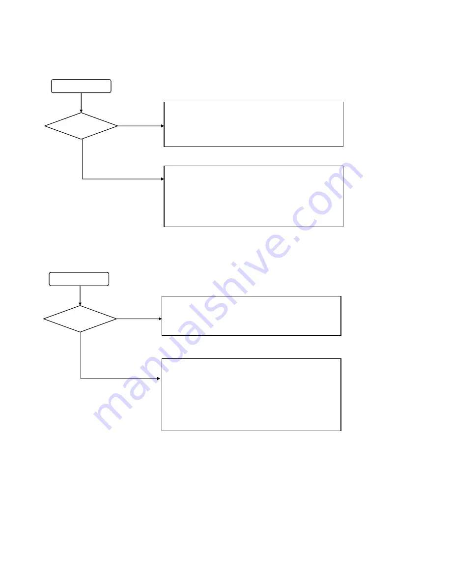
Component signal
is missing
Component screen
has no signal
Normal RGB output
yes
no
no
yes
Normal RGB port
No Pr signal : Check whether the signal is flown or not
J118.13-> F111-> R472 -> C474 -> IC152.7
Check whether R431 and R432 have bad soldering
No Pb signal : Check whether the signal is flown or not
J118.15-> F113-> R476 -> C476 -> IC152.8
Check whether R445 and R446 have bad soldering
Check whether L122 terminal is +9V
Check whether R507, R508, R244, R245 and R246 have bad
soldering
No Pr signal : Check whether there exists Q114.Base and
IC152.5 signals
No Pb signal : Check whether there exists Q116.Base and
IC152.10 signals
Check the direction of IC152 component
Check IC152.4 -> 9V, IC152.11 -> ground
Check whether L122 terminal is +9V
Check whether R507, R508, R244, R245 and R246 have bad
soldering
Check Y signal : Check whether there exists Q115.Base and
IC152.12 signals
Check Pr signal : Check whether there exists Q114.Base and
IC152.5 signals
Check Pb signal : Check whether there exists Q116.Base and
IC152.10 signals
Check the direction of IC152 component
Check IC152.4 -> 9V, IC152.11 -> ground
No Y signal : Check whether the signal is flown or not
J118.17-> F112-> R475 -> C475 -> IC152.14
Check whether R443 and R444 have bad soldering
Check the direction of IC152
Check IC152.4 -> 9V, IC152.11 -> ground
Summary of Contents for HDR230
Page 28: ......
Page 34: ......
Page 37: ......
Page 38: ...3 17 3 18 4 WAVEFORMS 1 DIGITAL SYSTEM CLOCK GENERATOR PART 1 2 3...
Page 39: ...3 19 3 20 2 DIGITAL SYSTEM SYSTEM MEMORY PART 1 2 3...
Page 40: ...3 21 3 22 3 VIDEO PLL PART 1 2...
Page 41: ...3 23 3 24 4 VIDEO OUTPUT CONNECTOR PART 1 2 3 BMK800 BMK800 BMK800 33PF 33PF 33PF...
Page 43: ...3 27 3 28 6 PVR CLOCK PART 1 2 3...
Page 44: ...3 29 3 30 7 VSB VSB DECODER PART 1...
Page 45: ...3 31 3 32 8 VSB DOWN CONVERTER PART 1...
Page 46: ...3 33 3 34 9 MICOM DOWN CONVERTER PART 1...
Page 47: ......
Page 65: ...3 74 3 75 10 VSB CIRCUIT DIAGRAM IF VSB TP Data clock error valid 03 3 15 HDR230 DNS...
Page 67: ...3 78 3 79 12 POWER IF COM VIDEO CIRCUIT DIAGRAM CVBS OUT Y OUT C OUT 03 3 15 HDR230...
Page 68: ...3 80 3 81 13 FRONT CIRCUIT DIAGRAM RIGHT LEFT 03 3 15 HDR230...
Page 69: ...3 82 3 83 8 PRINTED CIRCUIT DIAGRAMS 1 DIGITAL MAIN PRINTED CIRCUIT DIAGRAMS TOP...
Page 70: ...3 84 3 85 2 DIGITAL MAIN PRINTED CIRCUIT DIAGRAMS BOTTOM...
Page 72: ...3 88 3 89 5 POWER PRINTED CIRCUIT DIAGRAM LOCATION GUIDDE...


