- 4-15 -
DECK MECHANISM ADJUSTMENT
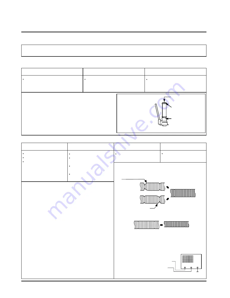
4.Guide Roller Height Adjustment
Adjustment Procedure
1) Confirm if the tape runs along the tape guide line of the
Lower Drum.
2) If the tape runs the bottom of the guide line, turn the
Guide Roller Height Adjustment Screw to clockwise
direction.
3) If it runs the top, turn to counterclockwise direction.
4) Adjust the height of the Guide Roller to be guided to the
guide line of the Lower Drum from the starting and end-
ing point of the Drum.
Purpose: To regulate the height of the tape so that the bottom of the tape runs along the
tape guide line on the Lower Drum.
Test Equipment/ Fixture
Post Height Adjusting Driver
Test Conditions (Mechanism Condition)
Play or Review Mode
Adjustment Point
Guide Roller Height Adjustment
screws on the Supply and Take-Up
Guide Rollers.
Fig. C-4-1
Upper Flange
Guide Roller
Retaining Screw
Guide Roller Height
Adjustment screw
ADJUSTMENT DIAGRAM
Test Equipment/Fixture
Oscilloscope
Alignment Tape
Post Height Adjusting
Driver
Test Equipment Connection Points
CH-1:PB RF Envelope
CH-2:NTSC: SW 30Hz
PAL: SW 25Hz
Head Switching Output
Point
RF Envelope Output
Point
Test Conditions VCR(VCP) State
Play an Alignment Tape
Adjustment Point
Guide Roller Height
Adjustment Screws
Fig. C-4-2
Fig. C-4-3
P3 POST
ADJUSTMENT
P2 POST
ADJUSTMENT
Turn the Roller Guide Height
Adjustment Screw slightly
to flatten the waveform.
Tracking Control at center
RF ENVELOPE OUTPUT TEST POINT
OSCILLOSCOPE
HEAD SWITCHING OUTPUT TEST
POINT
Turn(Move) the Tracking
Control to both directions
4-1. Preliminary Adjustment
4-2. Precise Adjustment
Adjustment Procedure
1) Play an Alignment Tape after connecting the probe of the
Oscilloscope to the RF Envelope Output Test Point and
Head Switching Output Test Point.
2) Tracking Control(in PB Mode) : Center Position(When
this adjustment is performed after the Drum Assembly
has been replaced, set the Tracking Control so that the
RF Output is Maximum).
3) Height Adjustment Screw : Flatten the RF waveform.
(Fig. C-4-2)
4) Turn(Move) the Tracking Control(in PB Mode) clockwise
and counterclockwise.(Fig. C-4-3)
5) Check that any drop of RF Output is uniform at the start
and end of the waveform.
NOTE
If the adjustment is excessive or insufficient the tape will
jam or fold.
Waveform Diagrams
Connection Diagram
Summary of Contents for XBS341 Series
Page 1: ...SERVICE MANUAL MODELS XBS341...
Page 10: ...2 1 SECTION 2 AUDIO PART...
Page 12: ...3 2 VCR ELECTRICAL TROULBESHOOTING...
Page 13: ...3 3...
Page 27: ...SECTION 4 MECHANSIM OF VCR PART...
Page 39: ...4 12...
Page 41: ...4 14...
Page 51: ...4 24...
Page 58: ...5 1 DVD ELECTRICAL TROUBLESHOOTING 1 Test debug flow SECTION 5 DVD PART...
Page 59: ...5 2...
Page 60: ...5 3...
Page 61: ...5 4...
Page 62: ...5 5...
Page 63: ...5 6...
Page 67: ...5 10 2 Tray close waveform 3 Tray open waveform...
Page 69: ...5 12 6 LASER POWER CONTROL RELATED SIGNAL NO DISC CONDITION 7 DISC TYPE JUDGEMENT WAVEFORM...
Page 70: ...5 13...
Page 71: ...5 14 8 FOCUS ON WAVEFORM...
Page 72: ...5 15 9 SPINDLE CONTROL WAVEFORM NO DISC CONDITION...
Page 73: ...5 16 10 TRACKING CONTROL RELATED SIGNAL System checking...
Page 74: ...5 17 11 RF WAVEFORM 12 MT1379 AUDIO OPTICAL AND COAXIAL OUTPUT ASPDIF...
Page 75: ...5 18 13 MT1379 VIDEO OUTPUT WAVEFORM 1 Full colorbar signal CVBS 2 Y...
Page 76: ...5 19 3 C 14 AUDIO OUTPUT FORM AUDIO DAC 1 Audio related Signal...
Page 77: ...5 20 MEMO...
Page 80: ...2 2 2 3 BLOCK DIAGRAM...
Page 81: ...2 4 2 5 AUDIO SHEMATIC DIAGRAMS U COM SCHEMATIC DIAGRAM...
Page 82: ...2 6 2 7 FUNCTION POWER SCHEMATIC DIAGRAM...
Page 83: ...2 8 2 9 MAIN AMP SCHEMATIC DIAGRAM...
Page 84: ...2 10 2 11 WIRING DIAGRAM...
Page 86: ...2 14 2 15 PRINTED CIRCUIT DIAGRAM MAINAMP FRONT P C BOARD SOLDER SIDE...
Page 87: ...2 16 2 17 MAINAMP FRONT P C BOARD COMPONENT SIDE...
Page 88: ...2 18 2 19 FUNCTION POWER P C BOARD SOLDER SIDE...
Page 89: ...2 20 2 21 FUNCTION POWER P C BOARD COMPONENT SIDE...
Page 90: ...3 17 3 18 VCR SHEMATIC DIAGRAMS SYSTEM SCHEMATIC DIAGRAM...
Page 91: ...3 19 3 20 A AUDIO V VIDEO SCHEMATIC DIAGRAM...
Page 93: ...3 23 3 24 HIFI TUNER SCHEMATIC DIAGRAM...
Page 94: ...3 25 3 26 A V JACK SCART SCHEMATIC DIAGRAM...
Page 96: ...3 29 3 30 PRINTED CIRCUIT DIAGRAMS TUNER P C BOARD...
Page 97: ...3 31 3 32 VCR P C BOARD...
Page 98: ...3 33 3 34 VCR P C BOARD...
Page 99: ...5 22 5 21 DVD PART SCHEMATIC DIAGRAMS MPEG SCHEMATIC DIAGRAM...
Page 100: ...5 23 5 24 SERVO SCHEMATIC DIAGRAM...
Page 101: ...5 25 5 26 AUDIO SCHEMATIC DIAGRAM...
Page 102: ...5 27 5 28 INTERFACE SCHEMATIC DIAGRAM...
Page 103: ...5 29 5 30 VOLTAGE SHEET IC TR...
Page 104: ...5 31 5 32 PRINTED CIRCUIT DIAGRAM DVD P C BOARD SOLDER SIDE...
Page 105: ...5 33 5 34 DVD P C BOARD COMPONENT SIDE...
Page 107: ...MEMO MEMO...
Page 109: ...MEMO MEMO...
Page 115: ......


