User Manual
This document is not allowed to
transmit without ZTE Corporation
’s
permission
©ZTE CORPORATION All rights reserved
19
4
Interf ace circuit design
The chapter provides the reference design on the interface circuit according to the module’s
functions and describes the precautions.
4.1
Reset and power design
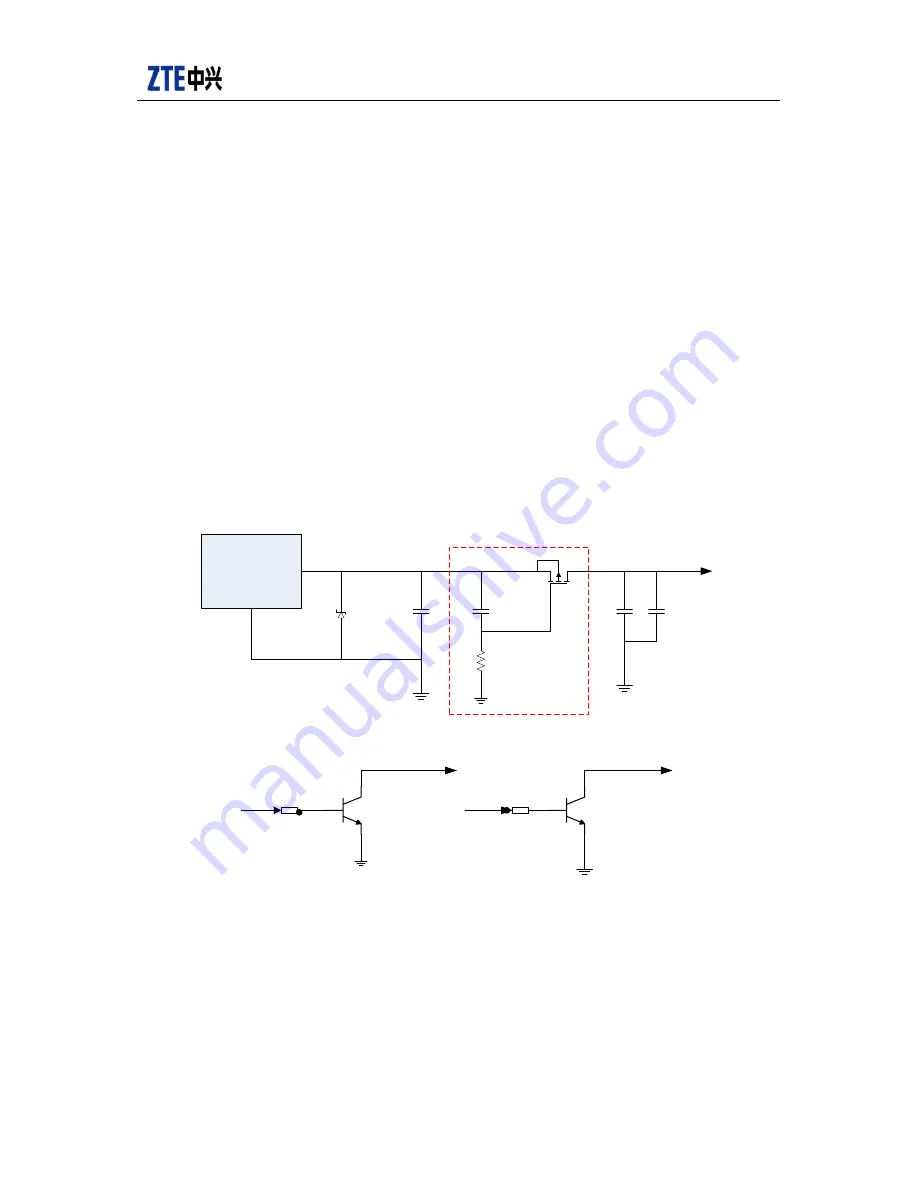
See the reference design principle of power and reset circuit in figure 4-1. Select appropriate
parameters according to the actual selected power supply since VD1 is TVS tube, and select CJ2305
from Changjiang Electronics or DMP2305U-7 from DIODES since VT1 is MOS tube. Refer to figure 4-2
for the design of power circuit. Select MIC29302 and adjust the output voltage through the
adjustment of R5 and R6. Please refer to MIC29302’s specification for detailed parameters design.
Please note that the components in the figure are just for your reference. For details, please adjust
according to the actual circuit.
Figure 4-1 Power & reset circuit reference design principle diagram
电源
VD1
TVS
C1
C2
22uf
C3
100uf
VT1
R1
15k
输出模块用电压
VBAT
C4
0.1uf
缓启动电路
MCU_ON/OFF
R2
4.7K
MCU_RESET
SYSRST_N
PWRKEY_N
R3
4.7K


