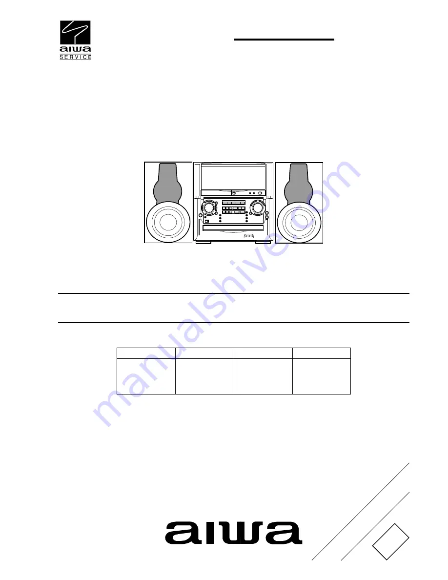
background image

SERVICE  MANUAL

DA

TA

COMPACT DISC

STEREO SYSTEM

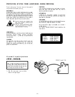
BASIC TAPE MECHANISM : 6ZM-1 AR3NM
BASIC CD MECHANISM : AZG-1 YZD3RDM

XH-A1000

EZ,K

S/M Code No. 09-006-421-4R2

REVISION

• This Service Manual is the “Revision Publishing” and replaces “Simple Manual”

XH-A1000 (EZ,K), (S/M Code No. 09-005-421-4T2).

• If requiring information about the CD mechanism, see Service Manual of AZG-1

(S/M  Code No. 09-001-335-3N8).

XH–A1000

RC–AAS01

SYSTEM

CD

SPEAKERS

REMOTE

CX–A1000

SX–WA1000

SX-C1800

SX–R1800

Summary of Contents for XH-A1000

Page 1: ...ode No 09 006 421 4R2 R E V I S I O N This Service Manual is the Revision Publishing and replaces Simple Manual XH A1000 EZ K S M Code No 09 005 421 4T2 If requiring information about the CD mechanism see Service Manual of AZG 1 S M Code No 09 001 335 3N8 XH A1000 RC AAS01 SYSTEM CD SPEAKERS REMOTE CX A1000 SX WA1000 SX C1800 SX R1800 ...

Page 2: ...MP 28 SCHEMATIC DIAGRAM 8 LOW AMP 29 WIRING 5 5CH AMP 30 SCHEMATIC DIAGRAM 9 5CH AMP 31 WIRING 6 VIDEO I O VIDEO JACK VIDEO 3 SCART 32 SCHEMATIC DIAGRAM 10 VIDEO I O VIDEO JACK VIDEO 3 CONNECT 3 3 33 SCHEMATIC DIAGRAM 11 SCART 34 WIRING 7 TUNER 35 SCHEMATIC DIAGRAM 12 TUNER 36 WIRING 8 PT 37 SCHEMATIC DIAGRAM 13 PT 38 WIRING 9 DECK DECK MOTOR HEAD 39 FL BJ733GK GRID ASSIGNMENT ANODE CONNECTION PIN...

Page 3: ...aker of 8 ohms or more PHONES stereo jack accepts headphones of 32 ohms or more Cassette deck section Track format 4 tracks 2 channels stereo Frequency response CrO2 tape 50 Hz 16000 Hz Normal tape 50 Hz 15000 Hz Signal to noise ratio 60 dB Dolby B NR ON CrO2 tape peak level above 400 Hz Recording system AC bias Heads Recording playback head x 1 erase head x 1 Compact disc player section Laser Sem...

Page 4: ...araten används på annat sätt än vad som specificeras i denna bruksanvising kan användaren utsättas för osynling laserstrålning som överskrider gränsen för laserklass 1 PROTECTION OF EYES FROM LASER BEAM DURING SERVICING CAUTION Use of controls or adjustments or performance of proce dures other than those specified herin may result in hazardous radiation exposure ATTENTION L utillisation de command...

Page 5: ...in power 2 2 2 2 2 Confirm that the main power is turned on and the HOLD terminal of the MICROCOMPUTER keeps the H level or not 3 3 3 3 3 When the HOLD terminal is L level the abnormality detection circuit is judged to be working correctly and the MICROCOMPUTER is judged to be good 1 Forced discharge of electrolytic capacitor of power supply block When repair is going to be attempted in the set th...

Page 6: ... ends of the electrolytic capacitor C113 that is connected to VDD of the MICROCOMPUTER with tweezers 3 3 3 3 3 Connect the AC power cord again If the MICROCOMPUTER returns to the normal operation the MICROCOMPUTER is good Note The reference number or MICROCOMPUTER pin number of transistor Q110 and electrolytic capacitor C113 can change depending on the models Be sure to check the reference numbers...

Page 7: ...isassembling procedure 3 Remove the 4 screws Ex2 Fx2 from both sides 1 Remove the 19 screws Ax11 Bx8 and remove the CABI STEEL 2 Remove the 3 screws from the bottom of the unit A A A A A A A B B B B B B CABI STEEL B B E F E F A A A A ...

Page 8: ...with the AZG 1 8 Remove the 2 screws and remove the AZG 1 from the CHAS 3CD The AZG 1 can be repaired while the power is on by using the jig introduced in the Service Technical Information SI 98 028 1 Procedure Connect the jig as shown below CD service position C C C C D C C C C C CABI REAR ASSY C C C D C C C C C C PWB CONNECT PANEL REAR CD CHAS 3CD CHAS 3CD AZG 1 ...

Page 9: ... FMB G16L 87 A40 345 080 ZENER MTZJ10C 87 070 136 080 ZENER MTZJ5 1B 87 A40 437 080 ZENER MTZJ4 3B 87 A40 349 080 ZENER MTZJ7 5C MAIN C B C1 87 012 369 080 C CAP S 0 047 50F C2 87 012 369 080 C CAP S 0 047 50F C3 87 012 368 080 C CAP S 0 1 50 F C4 87 012 368 080 C CAP S 0 1 50 F C5 87 012 368 080 C CAP S 0 1 50 F C6 87 012 368 080 C CAP S 0 1 50 F C9 87 A11 939 090 CAP E 4700 35 C10 87 A11 939 090...

Page 10: ...56 080 CHIP CAP S 0 068 25B C419 87 010 260 080 CAP ELECT 47 25V C421 87 012 140 080 CAP 470P C422 87 012 140 080 CAP 470P C451 87 010 401 080 CAP ELECT 1 50V C452 87 010 401 080 CAP ELECT 1 50V C454 87 010 402 080 CAP ELECT 2 2 50V C457 87 010 196 080 CHIP CAPACITOR 0 1 25 C458 87 010 196 080 CHIP CAPACITOR 0 1 25 C461 87 010 544 080 CAP ELECT 0 1 50V C471 87 010 402 080 CAP ELECT 2 2 50V C481 87...

Page 11: ...N 13P JL BT CN2 87 A60 739 010 CONN 13P JL BT CN91 87 A60 619 010 CONN 2P V 2MM JMT CN351 87 A60 625 010 CONN 8P V 2MM JMT CN601 87 A60 138 010 CONN 13P V FE CN602 87 A60 131 010 CONN 6P V FE CN603 87 A60 142 010 CONN 17P V FE CN605 87 A60 189 010 CONN 16P TUC P16P B1 CN606 87 A60 621 010 CONN 4P V 2MM JMT CN607 87 A60 140 010 CONN 15P V FE CN608 87 A60 621 010 CONN 4P V 2MM JMT CNA1 8A NF8 653 01...

Page 12: ... C CAP S 330P 50 CH C183 87 010 197 080 CAP CHIP 0 01 DM C184 87 010 182 080 C CAP S 2200P 50 B C185 87 010 197 080 CAP CHIP 0 01 DM C186 87 010 182 080 C CAP S 2200P 50 B C401 87 010 196 080 CHIP CAPACITOR 0 1 25 C402 87 010 196 080 CHIP CAPACITOR 0 1 25 C403 87 010 319 080 C CAP S 56P 50 CH C404 87 010 319 080 C CAP S 56P 50 CH C405 87 010 319 080 C CAP S 56P 50 CH C406 87 010 322 080 C CAP S 10...

Page 13: ...K 55001 5CH AMP C B C403 87 010 405 080 CAP ELECT 10 50V C404 87 010 405 080 CAP ELECT 10 50V C405 87 010 186 080 CAP CHIP 4700P C406 87 010 186 080 CAP CHIP 4700P C407 87 010 405 080 CAP ELECT 10 50V C408 87 010 405 080 CAP ELECT 10 50V C409 87 010 322 080 C CAP S 100P 50 CH C410 87 010 322 080 C CAP S 100P 50 CH C411 87 010 260 080 CAP ELECT 47 25V C412 87 010 260 080 CAP ELECT 47 25V C413 87 A1...

Page 14: ...25 C719 87 012 286 080 CAP U 0 01 25 C720 87 012 195 080 C CAP U 100P 50CH C721 87 012 176 080 CAP 15P C722 87 012 176 080 CAP 15P C723 87 012 274 080 CHIP CAP U 1000P 50B C725 87 018 131 080 CAP TC U 1000P 50 KB C727 87 010 196 080 CHIP CAPACITOR 0 1 25 C728 87 010 248 080 CAP ELECT 220 10V C729 87 012 274 080 CHIP CAP U 1000P 50B C731 87 012 286 080 CAP U 0 01 25 C733 87 012 280 080 C CAP U 3300...

Page 15: ...F CN1 87 A61 110 010 CONN 9P V TID A CN2 87 A60 850 010 CONN 7P V VH CN5 87 099 674 010 CONN 2P V VA CN6 87 A60 937 010 CONN 2P V VH PR1 87 026 682 080 PROTECTOR 10A 491 SERIES 60V PR2 87 026 682 080 PROTECTOR 10A 491 SERIES 60V PR3 87 026 682 080 PROTECTOR 10A 491 SERIES 60V PR4 87 026 682 080 PROTECTOR 10A 491 SERIES 60V PR5 87 026 682 080 PROTECTOR 10A 491 SERIES 60V PR6 87 026 682 080 PROTECTO...

Page 16: ...ue of resistor Chip resistor Wattage Type Tolerance 1 16W 1 10W 1 8W 1608 2125 3216 5 5 5 CJ CJ CJ Form L W t 1 6 0 8 0 45 2 1 25 0 45 3 2 1 6 108 118 128 A A CHIP RESISTOR PART CODE 0 55 Resistor Code Dimensions mm Symbol 1 16W 1005 5 CJ 1 0 0 5 0 35 104 L t W ...

Page 17: ...CC5551 CSA1585 CSC4115 CSD655 KTA1266 KTC3198 B C E 2SB1370 B C E 2SA1235 2SC2714 2SC3052 2SC3326 CMBT5401 CMBT5551 DTA123EKA G D S 2SK2937 G D S 2SK3053 B C E 2SB1588 2SD2439 FN1016 FP1016 G D S 2SK2158 2SJ561 T1 DTA123JK KTA1298 RT1N141C RT1P141C RT1P144C RT1P441C ...

Page 18: ...WIRING 1 MAIN FAN 18 10 11 12 13 14 15 16 17 18 19 20 21 22 23 24 A B C D E F G H I J K L M N O P Q R S T U 1 2 3 4 5 6 7 8 9 25 26 27 28 29 30 31 32 ...

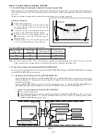
Page 19: ... 19 SCHEMATIC DIAGRAM 1 MAIN 1 4 AMP SECTION CONNECT 1 3 ...

Page 20: ... 20 SCHEMATIC DIAGRAM 2 MAIN 2 4 POWER SUPPLY SECTION ...

Page 21: ... 21 SCHEMATIC DIAGRAM 3 MAIN 3 4 DECK SECTION ...

Page 22: ... 22 SCHEMATIC DIAGRAM 4 MAIN 4 4 PRO LOGIC SECTION ...

Page 23: ... 23 SCHEMATIC DIAGRAM 5 FAN ...

Page 24: ...WIRING 2 FRONT CONNECT 24 10 11 12 13 14 15 16 17 18 19 20 21 22 23 24 A B C D E F G H I J K L M N O P Q R S T U 1 2 3 4 5 6 7 8 9 25 26 27 28 29 30 31 32 ...

Page 25: ... 25 SCHEMATIC DIAGRAM 6 FRONT CONNECT 2 3 DECK DECK MOTOR ...

Page 26: ...WIRING 3 OPERATE KEY MIC LED A D 26 10 11 12 13 14 15 16 17 18 19 20 21 22 23 24 A B C D E F G H I J K L M N O P Q R S T U 1 2 3 4 5 6 7 8 9 25 26 27 28 29 30 31 32 ...

Page 27: ... 27 SCHEMATIC DIAGRAM 7 OPERATE KEY MIC LED A D ...

Page 28: ...WIRING 4 LOW AMP 28 10 11 12 13 14 15 16 17 18 19 20 21 22 23 24 A B C D E F G H I J K L M N O P Q R S T U 1 2 3 4 5 6 7 8 9 25 26 27 28 29 30 31 32 ...

Page 29: ... 29 SCHEMATIC DIAGRAM 8 LOW AMP ...

Page 30: ...WIRING 5 5CH AMP 30 10 11 12 13 14 15 16 17 18 19 20 21 22 23 24 A B C D E F G H I J K L M N O P Q R S T U 1 2 3 4 5 6 7 8 9 25 26 27 28 29 30 31 32 ...

Page 31: ... 31 SCHEMATIC DIAGRAM 9 5CH AMP ...

Page 32: ...WIRING 6 VIDEO I O VIDEO JACK VIDEO 3 SCART 32 10 11 12 13 14 15 16 17 18 19 20 21 22 23 24 A B C D E F G H I J K L M N O P Q R S T U 1 2 3 4 5 6 7 8 9 25 26 27 28 29 30 31 32 ...

Page 33: ... 33 SCHEMATIC DIAGRAM 10 VIDEO I O VIDEO JACK VIDEO 3 CONNECT 3 3 ...

Page 34: ... 34 SCHEMATIC DIAGRAM 11 SCART ...

Page 35: ...WIRING 7 TUNER 35 10 11 12 13 14 15 16 17 18 19 20 21 22 23 24 A B C D E F G H I J K L M N O P Q R S T U 1 2 3 4 5 6 7 8 9 25 26 27 28 29 30 31 32 ...

Page 36: ... 36 SCHEMATIC DIAGRAM 12 TUNER ...

Page 37: ...WIRING 8 PT 37 10 11 12 13 14 15 16 17 18 19 20 21 22 23 24 A B C D E F G H I J K L M N O P Q R S T U 1 2 3 4 5 6 7 8 9 25 26 27 28 29 30 31 32 ...

Page 38: ... 38 SCHEMATIC DIAGRAM 13 PT ...

Page 39: ...WIRING 9 DECK HEAD DECK MOTOR 39 10 11 12 13 14 15 16 17 18 19 20 21 22 23 24 A B C D E F G H I J K L M N O P Q R S T U 1 2 3 4 5 6 7 8 9 25 26 27 28 29 30 31 32 ...

Page 40: ... 40 FL BJ733GK GRID ASSIGINMENT ANODE CONNECTION PIN CONNECTION ...

Page 41: ... 41 FL BJ734GK GRID ASSIGINMENT ANODE CONNECTION PIN CONNECTION ...

Page 42: ...IC BLOCK DIAGRAM 42 ...

Page 43: ... 43 ...

Page 44: ...t 3 22 I CDSW I CD tray position detect 23 I RTVR I Rotary encoder volume input 24 I JOG I Rotary encoder jog dial input 25 I TU SIG I MS I Tuner signal indicator input MS detect 26 I SPEANA I Spectrum analyzer level input 27 I TM BASE I Time base input for clock 28 I WRQ RDS CLK I CD WRQ input RDS clock input 29 I RMC I Remote commander signal input 30 O GON O FL grid driver control 31 O GSEL O F...

Page 45: ... CST O I FL segment driver output Cassette detect 65 P20 REB O I FL segment driver output Record enable switch B side detect 66 P19 CAM O I FL segment driver output Deck cam switch detect 67 P18 AUTO O I FL segment driver output Deck auto pulse detect 68 P17 REA O I FL segment driver output Record enable switch A side detect 69 71 P16 P14 O FL segment driver output 72 VDD4 5V supply 73 84 P13 P2 O...

Page 46: ...lows 9 FM SW O 2 BAND 3 BAND 3 BAND AM FM LW MW FM MW SW FM H L H H L H L L Outputs L or H as follows 10 MW SW O 2 BAND 3 BAND 3 BAND AM FM LW MW FM MW SW FM L L H L L L H L 11 IF MUTE O To control internal counter 12 IF IN I General purpose counter input 13 TUNE I Receives L when station is tuned 14 NC Not connected 15 AMIN I Receives the AM local oscillator frequency signal 16 FMIN I Receives th...

Page 47: ...Rs so that the output level at TP3 TP4 is 245mV 10 mV 5 REC PB Frequency Response Adjustment Settings Test tape TTA 602 NORMAL Test point TP3 Lch TP4 Rch Input signal 1kHz 10kHz 20VU Adjustment location SFR351 Lch SFR352 Rch Method Apply a 1kHz signal and REC mode Then adjust OSC attenuator so that the output level at the TP3 TP4 becomes 17mV Record and play back the 1kHz and 10kHz signals and adj...

Page 48: ...Hz is adjusted to MAX by TC942 6 AM IF Adjustment Settings Test point TP8 Lch TP9 Rch Adjustment location L772 450kHz 7 FM VT Check Settings Test point TP1 VT Method Set to FM 108 0MHz and check that the test point is less than 8 0V Then set to FM 87 5MHz and check that the test point is more than 0 5V 8 FM Tracking Check Settings Test point TP8 Lch TP9 Rch Method Set to FM 98 0MHz and check that ...

Page 49: ... 23 24 25 26 27 28 29 30 31 55 32 AZG 1 ZD8RNDM 34 56 35 60 63 36 37 38 F F F F F F F C J I J J J I F F F F F A H G H A A A F F F F F F F F F F F B B F F B F B F F F F A A E A F F D F F F F F D F 39 40 71 41 42 43 64 66 67 69 68 14 65 44 45 46 47 48 49 58 g 50 51 52 53 70 70 54 HT SINK TR HT SINK TR HT SINK MAIN 6ZM 1 AR3NM PT1 33 11 57 a a c c d d b g e f k j j k f e FL202 61 F F F F F J J b ...

Page 50: ... 47 8A MTM 223 010 JOINT CABI 2 48 8A MTM 041 010 PANEL TRAY DECK 49 88 906 701 110 FF CABLE 6P 1 25 700MM 50 8A MTM 204 010 HLDR DECK 51 87 NF4 221 010 HLDR CABLE 52 8A MTM 207 010 HLDR HT SINK B 53 8A MTM 206 010 HLDR HT SINK A 54 8A MTM 005 010 CABI STEEL 55 8A MTM 031 010 KNOB RTRY VOL 56 87 MA3 062 010 FOOT H17 57 84 ZG1 245 210 CAP OPTICAL 58 8A MTM 205 010 HLDR PWB MAIN 59 8A MTM 056 010 RE...

Page 51: ... 51 TAPE MECHANISM EXPLODED VIEW 1 2 a 6ZM 4 R3 P C B a 1 2 3 4 5 BASE MECHA 6 7 8 9 10 11 12 13 B A C C ...

Page 52: ...L1 202 010 FRAME CAS 5 86 ZL1 209 010 LEVER LOCK 6 86 ZL1 214 010 SPR P CAS 7 86 ZL1 211 010 ARM CLAMP 8 86 ZL1 206 010 GEAR TRAY 9 86 ZL1 213 010 SPR E CLAMP 10 86 ZL1 208 010 LEVER SW 11 86 ZL1 207 010 GEAR PULLEY 12 86 ZL1 212 010 BELT L 13 86 ZL1 210 010 PULLEY MOT A 83 ZG3 217 010 S SCREW GEAR D B 87 251 072 410 U 2 6 5 C 87 067 660 010 BVT2 3 8 W 0 SL0T BLK ...

Page 53: ...9 4 6 20 5 21 21 24 25 26 29 29 27 28 3 2 P C B HLDR WIRE 3 SHAFT REEL 18 B B A A B A B 31 38 39 40 32 34 33 35 43 45 41 41 37 44 50 P C B SOL1 49 47 48 46 C C E 36 42 52 51 55 CUSH G DIA 3 7 9 3 2 PLATE SHLD SH 1 75 3 6 0 5 SLT SH 1 63 3 2 0 5 SLT 53 54 22 8 22 8 C C C D D G H F ...

Page 54: ... ASSY PINCH R3 28 82 ZM1 259 110 SPR T PINCH R 29 82 ZM1 240 110 LVR REC 30 82 ZM1 298 010 SPR P EARTH 31 82 ZM1 255 310 SPR E LVR DIR 32 82 ZM1 221 110 GEAR CAM 33 82 ZM1 227 210 LVR TRIG 34 82 ZM1 224 410 LVR FR 35 86 ZM4 201 010 SPR E TRIG 3 36 82 ZM1 239 010 CAPSTAN 2 2 41 7 37 82 ZM1 223 010 GEAR PLAY 38 82 ZM1 322 010 SPR T FR 60 39 82 ZM1 220 210 GEAR IDLER 40 82 ZM1 316 010 RING MAGNET 3 4...

Page 55: ...rning to clockwise direction until click sound comes out Remove the grill frame and four pieces of rubber caps by pulling out with a flat bladed screwdriver Remove the screws from hole where installed rubber caps Insert a flat bladed screwdriver into the position indicated by the arrows and remove the panel Re move the screws of each speaker unit and then remove the speaker units TOOLS 1 Plastic h...

Page 56: ... 60 8 88 MS1 608 010 SPKR CERAMIC 9 88 NS5 611 010 CORD SPKR B L 10 88 MS1 610 010 CORD SPKR SPEAKER PARTS LIST SX CR1800 YSC NOTE This SX CR1800 Speaker contains SX C1800 Center Speaker and SX R1800 Rear Speaker DESCRIPTION REF NO KANRI NO PART NO 1 8A AS4 602 010 SPKR 100 C1800 1 8A AS5 601 010 SPKR 100 R1800 2 8A AS4 005 010 TERMINAL ASSY C1800 2 8A AS5 005 010 TERMINAL ASSY R1800 3 8A AS4 001 ...

Page 57: ...M 905 010 IB K E M K 1 8A MTM 906 010 IB EZ 9L M EZ 2 87 043 106 010 ANT FM 1007AWG 3 87 A90 030 010 ANT LOOP AM NC C 4 8A MTM 701 010 RC UNIT RC AAS01 ACCESSORIES PACKAGE LIST DESCRIPTION REF NO KANRI NO PART NO ...

Page 58: ...2 11 IKENOHATA 1 CHOME TAITO KU TOKYO 110 JAPAN TEL 03 3827 3111 Printed in Singapore 9620450 0251431 ...

Reviews: