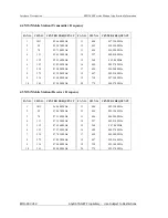
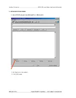
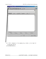
background image


Interface Description                                                                EMII-800 Service Manual Application Information


EMII-800 V1.0                                                  AnyDATA.NET Proprietary 

 Use Subject to Restrictions 


800M CDMA Wireless Kit 

                EMII-800   


AnyDATA.NET Inc. 

Hanvit Bank B/D 6F 

Byulyang-dong Kwachon 

KOREA 

                                                              Tel) 82-2-504-3360 

Fax) 82-2-504-3362 


SERVICE MANUAL 

Summary of Contents for EMII-800

Page 1: ...anual Application Information EMII 800 V1 0 AnyDATA NET Proprietary Use Subject to Restrictions 800M CDMA Wireless Kit EMII 800 AnyDATA NET Inc Hanvit Bank B D 6F Byulyang dong Kwachon KOREA Tel 82 2 504 3360 Fax 82 2 504 3362 SERVICE MANUAL ...

Page 2: ... or loss caused by the deletion or loss of data as a result of malfunctions or repairs The information disclosed herein is the exclusive property of AnyDATA NET Inc and no part of this publication may be reproduced or transmitted in any form or by any means including electronic storage reproduction adaptation translation execution or transmission without the prior written consent of AnyDATA NET In...

Page 3: ... s authority to operate the equipment To satisfy FCC RF exposure compliance requirements for a mobile transmitting device this device and its antenna should generally maintain a separation distance of 20cm or more from a person s body Special accessories In order to ensure this device in compliance with FCC regulation the special accessories are provided with this device and must be used with the ...

Page 4: ...CDMA Module 4 3 Structure and Functions of CDMA Module 7 4 Specification 8 CHAPTER 2 NAM Input Method Inputting of telephone numbers included 1 NAM Programming Method and Telephone Number Input Method 11 CHAPTER 3 Circuit Description 1 Overview 14 2 RF Transmit Receive Part 14 3 Digital Voice Processing Part 17 4 Level Translator Part 24 CHAPTER 4 FCC Notice Appendix 22 1 Assembly and Disassembly ...

Page 5: ...tly used Soft Softer Handoff Hard Handoff and Dynamic RF power Control technologies are combined into this phone to reduce the call being interrupted in a middle of talking over phone CDMA digital cellular network consists of MSC Mobile Switching Office BSC Base Station Controller BTS Base station Transmission System and MS Mobile Station Communication between MS and BTS is designed to meet the sp...

Page 6: ... multi access technology under the interference limited environment It can process more number of subscribers compared to other systems TDMA system has the processing capacity three times greater than the existing FDMA system whereas CDMA system about 12 15 times of that of the existing system CDMA system can be explained as follows TDMA or SDMA can be used to enable each person to talk alternatel...

Page 7: ... system capacity can be maximized If the signal of mobile station is received too strong the performance of that mobile station is improved However because of this the interference on other mobile stations using the same channel is increased and accordingly the call quality of other subscribers is reduced unless the maximum accommodation capacity is reduced In the CDMA system forward power control...

Page 8: ...nfidentiality CDMA signals have the function of effectively protecting call confidentiality by spreading and interleaving call information in broad bandwidth This makes the unauthorized use of crosstalk search receiver and radio very hard substantially Also included is the encryption function on various authentication and calls specified in IS 95 for the double protection of call confidentiality 2...

Page 9: ... classes For example the system operator can increase the number of channels available for use during the busy hour despite the drop in call quality This type of function requires 40 of normal call channels in the standby mode during the handoff support in an effort to avoid call disconnection resulting from the lack of channels In addition in the CDMA system services and service charges are class...

Page 10: ...st adjacently located is demodulated in order to obtain the sequence of encoded data symbols During the operation with one cell site the searcher searches out multi paths in accordance with terrain and building reflections On three data receivers the most powerful four paths are allocated for the parallel tracing and receiving Fading resistance can be improved a great deal by obtaining the diversi...

Page 11: ...12V 4 1 4 Operating Temperature 30 60 4 1 5 Frequency Stability CDMA 300 Hz 4 1 6 Antenna Whip Type 50 Ω 4 1 7 Size and Weight 1 Size 121mm x 57mm x 24mm L x W x D with case 2 Weight 112g 4 1 8 Channel Spacing CDMA 1 25MHz 4 2 Receive Specification 4 2 1 Frequency Range Digital 869 04 MHz 893 97 MHz 4 2 2 Local Oscillating Frequency Range 966 88MHz 12 5MHz 4 2 3 Intermediate Frequency 85 38MHz 4 2...

Page 12: ...ncy Range 966 88 MHz 12 5 MHz 4 3 3 Intermediate Frequency 130 38 MHz 4 3 4 Output Power 0 32W 4 3 5 Interference Rejection 1 Single Tone 101dBm with Jammer of 30dBm at 900 kHz 2 Two Tone 101dBm with Jammer of 43dBm at 900 kHz 1700kHz 4 3 7 CDMA TX Frequency Deviation 300Hz or less 4 3 8 CDMA TX Conducted Spurious Emissions less than 42 dBc 30kHz 900KHz less than 54 dBc 30kHz 1 98MHz 4 3 9 CDMA Mi...

Page 13: ...17 18 19 20 404 445 486 527 568 609 650 697 738 779 837 120 MHz 838 350 MHz 839 580 MHz 840 810 MHz 842 04 MHz 843 270 MHz 844 500 MHz 845 910 MHz 847 140 MHz 848 370 MHz 4 5 MS Mobile Station Receiver Frequency FA NO CH NO CENTER FREQUENCY FA NO CH NO CENTER FREQUENCY 1 2 3 4 5 6 7 8 9 10 1011 29 70 111 152 193 234 275 316 363 869 640 MHz 870 870 MHz 872 100 MHz 873 330 MHz 874 560 MHz 875 790 MH...

Page 14: ...1 INSTALLATION METHOD IDLEBUSY SMS PWR i PORT AnyDATA 6 12V Input UART1 EAR MIC UART2 ANT Connector COM1 8 Pin to 9 Pin Cable Power Supply 6 12V HeadSet ANT 1 Supply the voltage of 6 12V to 2pin Connector of the EMII 800 2 Connect the UART1 to PC COM1 port with the RS 232C cable 3 Install the operating program CHAPTER 2 NAM Input Method ...

Page 15: ...MII 800 Service Manual Application Information EMII 800 V1 0 AnyDATA NET Proprietary Use Subject to Restrictions 2 OPERATION METHOD 2 Set Buad rate to the modem s 3 Click DM mode 1 Run PSTDM program at Windows95 or Windows98 ...

Page 16: ...n EMII 800 Service Manual Application Information EMII 800 V1 0 AnyDATA NET Proprietary Use Subject to Restrictions 4 If OK is displayed in the message box modem is now ready for communication with PC 5 Click MENU BAR icon ...

Page 17: ... be displayed See if clock is running If it isn t communication with PC is not activated Repeat step 1 through 5 or reset the power of modem and repeat step 1 through 5 7 Type NAM Programming script like the example shown below NAM Programming script example Mode offline d ENTER nv_write name_nam 0 AnyDATA telecom ENTER nv_write name_nam 1 AnyDATA telecom ENTER Mode reset ENTER SCRIPTINPUT WINDOW ...

Page 18: ...difference generated between reference clocks In the signals coming out from the output terminal of DAC there are spurious frequency ingredients resulting from DAC output transition edge and parasite ingredients transmit clock frequencies and harmonics which are unwanted signals Accordingly spurious ingredients are removed by passing the signals through LPF of passband 6 30KHz Unlike the receive e...

Page 19: ...ter FL101 Transmit signals that have been converted from IF signals into RF signals after passing through the upconverter U105 are inputted into the Power Amp U103 after passing once again through RF BPF F101in order to filter out noise signals amplified during the amplification of RF signals after going through upconverter U105 This is carried out in order to create power level inputted to the Po...

Page 20: ...MHz 1200MHz and IF band 20MHz 300MHz U202 that receives the reference frequency of 19 68MHz from U174 creates 30kHz comparison frequency with the use of internal program and then changes the frequency of 900MHz band inputted from X200 which is the voltage adjustment crystal oscillator into the comparison frequency of 30kHz at the prescaler in U202 Then two signal differences are calculated from th...

Page 21: ...ce signals amplifying part for amplifying the voice signals and sending them to the ear piece amplifying part that amplifies ringer signals coming out from MSM5100 and amplifying part that amplifies signals coming out from MIC and transferring them to the audio processor 3 2 2 MSM Mobile Station Modem Part MSM is the core elements of CDMA terminal and carries out the functions of CPU encoder inter...

Page 22: ...trols the terminal operation Digital voice data that have been inputted are voice encoded and variable rated Then they are convolutionally encoded so that error detection and correction are possible Coded symbols are interleaved in order to cope with multi path fading Each data channel is scrambled by the long code PN sequence of the user in order to ensure the confidentiality of calls Moreover bi...

Page 23: ...d 2 7V The generated voltages are used for MSM5100 RFT3100 IFR3000 and other LOGIC parts PWR ASIC is operated by the control signal SLEEP from MSM5100 and POWER_EN signal 3 3 4 Logic Part The Logic part consists of internal CPU of MSM MCP The MSM5100 receives TCXO 19 68Mz from VC TCXO and CHIPX8 clock signals from the IFR3000 and then controls the module during the CDMA and the FM mode The major c...

Page 24: ...d All the control signals of the RS 232 signals are active low but data signals of RXD and TXD are active high The UART has a 64byte transmit TX FIFO and a 64byte receive RX FIFO The UART Features hardware handshaking programmable data sizes programmable stop bits and odd even no parity The UART operates at a 115 2kbps maximum bit rate 4 2 1 UART Inter Pinouts NAME DESCRIPTION CHARACTERISTIC DP_DC...

Page 25: ... Vout 2 8V 3V 3V MSM_input MSM_output SIPEX207 4V V EMII 800 02 04 RS232 PHONE TX01 RX02 TX04 RX03 VMAX 7 68V VMIN 7 68V VMAX 6 50V VMIN 6 64V VMAX 3 00V VMIN 0V VMAX 3 9V VMIN 0V Figure 4 2 Signal Level of RXD TXD 4 3 The function of Real Audio Test including Voice Test NAME TYPE DESCRIPSION MIC I Microphone audio input MIC IS Ear microphone set detect EAR O Ear audio output GND_A Audio ground ...

Page 26: ...the instructions may cause harmful interference to radio communications However there is no guarantee that interference will not occur in a particular installation If this equipment does cause harmful interference to radio or television reception which can be determined by turning the equipment off and on the user is encouraged to try to correct the interference by one or more of the following mea...

Page 27: ...ption EMII 800 Service Manual Application Information EMII 800 V1 0 AnyDATA NET Proprietary Use Subject to Restrictions 1 Assembly and Disassembly Diagram 2 Block Circuit Diagram 3 Part List 4 Component Layout APPENDIX ...

Page 28: ...MII 800 Service Manual Application Information EMII 800 V1 0 AnyDATA NET Proprietary Use Subject to Restrictions 1 Assembly and Disassembly Diagram DC6 12V INPUT RS232C IDLE BUSY SMS PWR EAR MIC DEBUG CDMA ANT i PORT AnyDATA ...

Page 29: ...rface Description EMII 800 Service Manual Application Information EMII 800 V1 0 AnyDATA NET Proprietary Use Subject to Restrictions 2 Block Circuit Diagram 2 1 MODEM Block Diagram 2 2 EMII 800 Block Diagram ...

Page 30: ... RFT3100 32BCCP TR RFT3100 32P BOT U102 1 QUALCOMM 4 MB84VD21182A 85 PBS MCP 16M 4M BOT U505 1 FUJITSU 5 MIC5245 3 0VBM5 LDO 3 0V TOP U601 U602 U604 U603 U607 5 MICREL 6 MIC5245 2 7VBM5 LDO 2 7V BOT U606 1 MICREL 7 TC7SU04FU INVERTER TOP U205 1 TOSHIBA 8 FDC634P P CH MOSFET SSOT 6 BOT U104 1 FAIRCHILD 9 S 80827ALNP EDT T2 RESET IC TOP U608 U609 1 SEIKO TOP Q302 Q307 Q303 Q305 Q304 5 ROHM 10 DTC124...

Page 31: ...1 1 SUNRIDGE 14 HSMP 389F DOIODE TOP Q107 1 AGILENT INDUCTOR 1 0603CS 30NXG BC 30N CHIP COIL 2 BOT L113 1 COILCRFT 2 0603CS 72NXG BC 72N CHIP COIL 2 TOP L203 1 COILCRFT 3 0603CS 180NXG BC 180N CHIP COIL 2 BOT L106 1 COILCRFT 4 0603CS 220NXG BC 220N CHIP COIL 2 TOP L114 1 COILCRFT 5 CI B1005 47NSJT IND 4 7N 5 BOT L201 1 CERATECH 6 CI B1005 82NSJT IND 8 2N 5 BOT L111 1 CERATECH 7 CI B1005 120NSJT IN...

Page 32: ...C403 3 MURATA TOP C109 1 MURATA 10 GRM36C0G220J50PT 22pF 1005 Cap BOT C129 1 MURATA 11 GRM36COG240J50PT 24pF 1005 Cap BOT C164 C165 2 MURATA 12 GRM36C0G680J50PT 68pF 1005 Cap BOT C142 1 MURATA TOP C211 C213 2 MURATA 13 GRM36C0G820J50PT 82pF 1005 Cap BOT C146 C151 2 MURATA TOP C100 C134 C418 C417 C108 C101 C103 7 MURATA 14 GRM36COG101J50PT 100pF 1005 Cap BOT C243 C241 C285 C280 C288 C230 C231 C232 ...

Page 33: ... BOT C287 C229 C286 C265 C228 C291 C226 C223 C222 C270 C424 C423 C428 C426 C120 C111 C191 C159 C160 C141 C131 C138 C166 20 MURATA TOP C105 C106 C116 C117 C456 4 24 GRM36COG105J50PT 1uF 1005 Cap BOT C247 1 MURATA 25 GRM39COG050J50PT 5pF 1608 Cap TOP C102 1 MURATA 26 GRM39COG101J50PT 100pF 1608 Cap TOP C501 1 MURATA TOP C253 1 MURATA 27 GRM39COG102J50PT 1nF 1608 Cap BOT C148 1 MURATA 28 GRM39Y5V103Z...

Page 34: ...10 R111 2 ROHM 10 MCR01MZSJX331 330W 5 1005 Resistor BOT R240 R402 2 ROHM 11 MCR01MZSJX471 470W 5 1005 Resistor BOT R361 R362 R365 R366 R363 R364 R360 R359 R358 R355 R357 R356 R353 R351 R354 R352 R349 R350 R347 R348 R346 R345 R343 R344 R341 R342 R329 R340 R327 R328 R325 R326 R323 R324 R321 R322 R319 R320 R301 R302 R318 R303 R308 R309 R304 R317 40 ROHM 12 MCR01MZSJX511 510W 5 1005 Resistor BOT R231...

Page 35: ...05 Resistor BOT R422 R423 2 ROHM 27 MCR01MZSJX474 470KW 5 1005 Resistor BOT R427 1 ROHM 28 MCR01MZSFX1212 12 1KW 1 1005 Resistor BOT R119 1 ROHM 29 MCR01MZSFX1003 100KW 1 1005 Resistor TOP R222 1 ROHM 30 MCR01MZSFX1503 150KW 1 1005 Resistor TOP R225 1 ROHM 31 MCR01MZSFX1004 1MW 1 1005 Resistor TOP R118 R117 2 ROHM 타 1 DTSS 1800 V0 3 PCB Main PCB 1 LGE 2 DTSS 1800 TOP COVER 구 TOP COVER 1 JUNG IL 3 ...

Page 36: ...LED Yellow TOP D1 D2 D3 3 BRT 11 HSJ1621 019011 EARJACK TOP U15 1 HOSIDEN 12 53047 0310 1 25mm male 3pin TOP CN10 1 MOLEX 13 5268 2 5mm male 3pin TOP CN2 1 MOLEX 14 5268 2 5mm male 2pin TOP J1 1 MOLEX RESISTOR 15 MCR03MZSJX000 RESISTOR 1608 0R TOP R30 R31 R44 R45 R46 R47 6 ROHM 16 MCR03MZSJX101 RESISTOR 1608 100R TOP R7 R8 R9 R34 R35 R36 R37 7 ROHM 17 MCR03MZSJX332 RESISTOR 1608 3 3K TOP R1 R2 R3 ...

Page 37: ...Y TOSUNG 27 EM FRONT 00 FRONT TOSUNG 28 EM REAR 00 REAR TOSUNG DNI 29 DNI RESISTOR TOP R4 R13 R14 R15 R16 R17 R18 R19 R20 R21 R22 R23 R24 R25 R26 R27 R40 R41 R42 R43 20 30 DNI CAPACITOR TOP C3 C4 2 31 DNI DA114 TOP D5 1 32 DNI INDUCTOR TOP L1 1 33 DNI MIC5205 3 0V TOP U4 1 34 DNI TC74HC07AF SOP 14 TOP U6 1 35 DNI TC74HC4052AFT SOP 16 TOP U5 1 36 DNI 53047 0810 8PIN TOP U7 1 37 DNI 5268 3PIN TOP CN...

Page 38: ...Interface Description EMII 800 Service Manual Application Information EMII 800 V1 0 AnyDATA NET Proprietary Use Subject to Restrictions 4 Component Layout ...

Reviews: