background image

SERVICE MANUAL

DV911SM

POWER

Summary of Contents for DV911SM

Page 1: ...SERVICE MANUAL DV911SM POWER ...

Page 2: ......

Page 3: ... removing an electrical assembly equipped with ES devices place the assembly on a conductive surface such as alminum foil to prevent electrostatic charge buildup or exposure of the assembly 3 Use only a grounded tip soldering iron to solder or unsolder ES devices 4 Use only an anti static solder removal device Some solder removal devices not classified as anti static ESD protected can generate ele...

Page 4: ...ront Panel Illustration POWER switch 2 Disc tray 3 4 5 6 PLAY button PAUSE STOP button 3 2 5 6 4 IR SENSOR button OPEN CLOSE button 7 8 7 8 MIC jack MIC VOLUME knob 9 9 VOL MIC POWER POWER indicator LED ...

Page 5: ...e installation the both ends of the laser diode are short circuited After replacing the parts with new ones remove the short circuit according to the correct procedure See this Technical Guide 2 Do not use a tester to check the laser diode for the optical pickup Failure to do so willdamage the laser diode due to the power supply in the tester 4 2 Handling precautions for Traverse Unit Optical Pick...

Page 6: ...5 1 Optical pickup Unit Explosed View and Part List Pic 1 ...

Page 7: ... MIDDLE A 1 7 1EA2511A29400 GEAR MIDDLE B 1 8 1EA2744A03000 SHAFT SLIDE 1 9 1EA2744A03100 SHAFT SLIDE SUB 1 10 1EA2812A15300 SPRING COMP TYOUSEI 3 11 1EA2812A15400 SPRING COMP RACK 1 21 1EA0B10B20100 ASSY PWB 1 Or 1EA0B10B20200 ASSY PWB 1 31 SEXEA25700 SPECIAL SCREW BIN M2X11 3 32 SEXEA25900 SPECIAL SCREW M1 7X2 2 2 33 SFBPN204R0SE SCR S TPG PAN 2X4 2 34 SFSFN266R0SE SCR S TPG FLT 2 6X6 1 35 SWXEA...

Page 8: ...lt wheel 17 Pick up 5 gearwheel 18 switch 6 iron chip 19 Five pin flat plug 7 Immobility mechanism equipment 20 screw 8 Magnet 21 PCB 9 Platen 22 motor 10 Bridge bracket 23 Motor wheel 11 screw 24 screw 12 screw 25 tray 13 Big bracket Before going process with disassembly and installation please carefully both peruse the chart and confirm the materials ...

Page 9: ...th a soldering iron after a circuit is connected Keep the power source of the pick up protected from internal and external sources of electrical noise Refrain from operation and storage in atmospheres containing corrosive gases such as H2S SO2 NO2 and Cl2 or toxic gases or in locations containing substances especially from the organic silicon cyan formalin and phenol groups which emit toxic gases ...

Page 10: ...Connect the oscilloscope to the video output terminal and terminate at 75 ohms 2 Confirm that luminance signal Y S level is 1000mVp p 30mV Measurement point Video output terminal Color bar 75 PLAY Title 46 DVDT S15 PLAY Title 12 DVDT S01 DVDT S15 or DVDT S01 Mode Disc Measuring equipment tools 200mV dir 10 sec dir 1000mVp p 30mV Confirmation value ...

Page 11: ...utput terminal and terminate at 75 ohme 2 Confirm that the chrominance signal C level is 621 mVp p 30mV Measurement point Video output terminal Color bar 75 PLAY Title 46 DVDT S15 PLAY Title 12 DVDT S01 DVDT S15 or DVDT S01 Mode Disc Measuring equipment tools Confirmation value Screwdriver Oscilloscope 200mV dir 10 sec dir 621mVp p 30mV ...

Page 12: ......

Page 13: ...tor Sectors can be locked in system or via programming equipment Temporary Sector Unprotect feature allows code changes in previously locked sectors Unlock Bypass Program Command Reduces overall programming time when issuing multiple program command sequences Top or bottom boot block configurations available Embedded Algorithms Embedded Erase algorithm automatically preprograms and erases the enti...

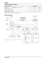
Page 14: ...ess time ns tACC 70 90 120 Max CE access time ns tCE 70 90 120 Max OE access time ns tOE 30 35 50 Input Output Buffers X Decoder Y Decoder Chip Enable Output Enable Logic Erase Voltage Generator PGM Voltage Generator Timer VCC Detector State Control Command Register VCC VSS WE BYTE CE OE STB STB DQ0 DQ15 A 1 Sector Switches RY BY RESET Data Latch Y Gating Cell Matrix Address Latch A0 A19 ...

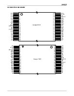
Page 15: ...Q12 DQ4 VCC DQ11 DQ3 DQ10 48 33 47 46 45 44 43 42 41 40 39 38 37 36 35 34 25 32 31 30 29 28 27 26 A1 A15 A18 A14 A13 A12 A11 A10 A9 A8 A19 NC WE RESET NC NC RY BY A17 A7 A6 A5 A4 A3 A2 1 16 2 3 4 5 6 7 8 17 18 19 20 21 22 23 24 9 10 11 12 13 14 15 A16 DQ2 BYTE VSS DQ15 A 1 DQ7 DQ14 DQ6 DQ13 DQ9 DQ1 DQ8 DQ0 OE VSS CE A0 DQ5 DQ12 DQ4 VCC DQ11 DQ3 DQ10 48 33 47 46 45 44 43 42 41 40 39 38 37 36 35 34 ...

Page 16: ... 22 RESET A18 A17 A7 A6 A5 A4 A3 A2 A1 A0 CE VSS OE DQ0 DQ8 DQ1 DQ9 DQ2 DQ10 DQ3 DQ11 44 43 42 41 40 39 38 37 36 35 34 33 32 31 30 29 28 27 26 25 24 23 WE A19 A8 A9 A10 A11 A12 A13 A14 A15 A16 BYTE VSS DQ15 A 1 DQ7 DQ14 DQ6 DQ13 DQ5 DQ12 DQ4 VCC SO A1 B1 C1 D1 E1 F1 G1 H1 A2 B2 C2 D2 E2 F2 G2 H2 A3 B3 C3 D3 E3 F3 G3 H3 A4 B4 C4 D4 E4 F4 G4 H4 A5 B5 C5 D5 E5 F5 G5 H5 A6 B6 C6 D6 E6 F6 G6 H6 DQ15 A ...

Page 17: ...r 16 bit mode CE Chip enable OE Output enable WE Write enable RESET Hardware reset pin RY BY Ready Busy output N A SO 044 VCC 3 0 volt only single power supply see Product Selector Guide for speed options and voltage supply tolerances VSS Device ground NC Pin not connected internally LOGIC SYMBOL 20 16 or 8 DQ0 DQ15 A 1 A0 A19 CE OE WE RESET BYTE RY BY N A SO 044 ...

Page 18: ...ance memory system applications 3 3V power supply LVTTL compatible with multiplexed address two banks operation MRS cycle with address key programs CAS Latency 2 3 Burst Length 1 2 4 8 full page Burst Type Sequential Interleave All inputs are sampled at the positive going edge of the system clock Burst Read Single bit Write operation DQM for masking Auto self refresh 32ms refresh period 2K cycle G...

Page 19: ...w column addresses are multiplexed on the same pins Row address RA0 RA10 column address CA0 CA7 BA Bank Select Address Selects bank to be activated during row address latch time Selects bank for read write during column address latch time RAS Row Address Strobe Latches row addresses on the positive going edge of the CLK with RAS low Enables row access precharge CAS Column Address Strobe Latches co...

Page 20: ...ation without notice Bank Select Data Input Register 512K x 16 512K x 16 Sense AMP Output Buffer I O Control Column Decoder Latency Burst Length Programming Register Address Register Row Buffer Refresh Counter Row Decoder Col Buffer LRAS LCBR LCKE LRAS LCBR LWE LDQM CLK CKE CS RAS CAS WE L U DQM LWE LDQM DQi CLK ADD LCAS LWCBR Timing Register ...

Page 21: ...egrates the MediaTek 2nd generation front end analog RF amplifier and the Servo MPEG AV decoder The progressive scan of the MT1389 utilized a proprietary advanced motion adaptive de interlace algorithm to achieve the best movie video playback It can easily detect 3 2 2 2 pull down source and restore the correct original pictures It also supports a patent pending edge preserving algorithm to remove...

Page 22: ... output or digital output Embedded Micro controller Built in 8032 micro controller Built in internal 373 and 8 bit programmable lower address port 1024 bytes on chip RAM Up to 4M bytes FLASH programming interface Supports 5 3 3 Volt FLASH interface Supports power down mode Supports additional serial port DVD ROM CD ROM Decoding Logic High speed ECC logic capable of correcting one error per each P ...

Page 23: ...ne echo Microphone tone control Vocal mute vocal assistant Key shift up to 8 keys Chorus Flanger Harmony Reverb Channel equalizer 3D surround processing include virtual surround and speaker separation TV Encoder Six 108MHz 12bit DACs Support NTSC PAL BDGHINM PAL 60 Support 525p 625p progressive TV format Automatically turn off unconnected channels Support PC monitor VGA Support Macrovision 7 1 L1 ...

Page 24: ...SEG7 KS7 17 SEG8 KS8 18 SEG9 KS9 19 SEG10 KS10 20 SEG11 21 SEG12 GR7 22 VDD 25 GND 26 GR5 24 GR4 27 GR3 28 GND 29 GR2 30 GR1 31 GND 32 U401 PT6961 LEDAT LEDCK LEDST KEY1 KEY2 KEY3 S1 S2 S3 S4 S5 S7 S10 G9 G8 G12 G6 VCC VCC VCC TC403 100uF 16V S11 R405 100R TC404 100uF 16V VCC G1 G2 G3 G4 G5 S6 G7 S8 S9 G10 G11 S12 5 4 3 2 1 12 11 10 9 8 7 6 LED 401 LED SOCK 1 C404 R407 R408 R406 TC401 OK L401 3 2 ...

Page 25: ......

Page 26: ...50V TC506 1000uF 10V TC505 1000uF 10V TC510 1000uF 10V D508 HER105 TC503 470uF 16V R511 330R 1W R507 1K R501 680K 2W D510 SR560 D506 HER105 D509 1N4007 D511 HER105 3 3V TC513 100uF 16V D503 1N4007 A 1 K 2 D502 1N4007 D504 1N4007 D501 1N4007 C508 104 C510 104 9V 5V ZD502 9 1V 1W VDD 4 D 5 S 2 FB 3 D 6 D 7 D 8 S 1 U501 VIPER22 R512 9 1K D513 1N4007 1 2 3 4 5 6 7 8 9 10 T501 EEL19H 9V GND 3 3V 5V GND...

Page 27: ......

Page 28: ...09 47uF 16V R629 27K 1 2 TC605 22U 16V TC603 4 7U 16V 9VA C619 102 R628 4 7K R620 10K R633 10R1 6W TC615 100U 16V C601 104 R632 10R1 6W TC616 100U 16V C602 104 9V 9VA 9V 9VA C622 104 C623 104 OKA TC610 4 7uF 16V TC613 4 7U 16V VDD 1 REF 2 AGND 3 DGND 4 CLKO 5 VCO 6 CC1 7 CC2 8 OP1 OUT 9 OP1 IN 10 OP2 IN 11 OP2 OUT 12 LPF2 IN 13 LPF2 OUT 14 LPF1 OUT 15 LPF1 IN 16 U603 PT2399 TC611 4 7U 16V 9VA TC62...

Page 29: ......

Page 30: ...09 330R R710 2 2K 10V A 10V AGND PDAT0 V703 8050 R711 1K R712 2 2K A 10V PDAT2 C716 104 AGND VCC AGND R707 A 10V AGND AGND VCC PDAT0 10V VGND VGND Pr L709 FBSMT L708 FBSMT L707 FBSMT Y1 Pb VGND GREEN BLUE RED B G R 1 2 3 4 5 6 JK702 RCA 407 BLACK TC702 1000uF 10V TC703 220uF 16V TC704 220uF 16V L710 FBSMT SPDIF R701 220R C710 104 L713 FCM L714 FCM C707 105 VGND R713 0R AGND VGND R703 68R VIN 1 VCC...

Page 31: ......

Page 32: ... A16 A15 A14 A13 A12 A11 A10 A9 A20 PCE A1 PRD AD0 AD1 AD2 AD3 AD4 AD5 AD6 A21 AD7 A17 A0 V18 VSCK VSDA VSTB SCL SDA RXD TXD URST IR DQM0 DQS0 DQ7 DQ6 DQ5 DQ4 DQ3 DQ2 DQ1 DQ0 DQ15 DQ14 R213 1K DQ9 DQ10 DQ11 DQ12 DQ13 DQ8 RAS CAS WE DQM1 LIMIT CS BA0 BA1 DMA10 DMA0 DMA1 DMA2 DMA3 DCLKB DMA9 DMA11 DCKE DCLK DMA8 DMA7 DMA6 DMA5 DMA4 DQ31 DQ27 DQ28 DQ29 DQ30 DQ26 DQ25 DQ24 DQM3 DQM2 DQ23 DQ22 DQ17 DQ1...

Page 33: ...203 10uF 16V A5VV VGND R222 0R DNS XI Q204 9016 RAS 17 CS 18 CAS 16 CKE 34 A0 21 A1 22 A2 23 A3 24 A4 27 A5 28 A6 29 A7 30 A8 31 A9 32 A10 20 BA A11 19 CLK 35 DQ7 12 DQ6 11 DQ5 9 DQ4 8 DQ3 6 DQ2 5 DQ1 3 DQ0 2 DQ8 39 DQ9 40 DQ10 42 DQ11 43 DQ12 45 DQ13 46 DQ14 48 DQ15 49 VCC 1 VCC 25 VCCQ 13 VCCQ 7 VCCQ 38 VCCQ 44 VSSQ 4 VSSQ 10 VSSQ 41 VSSQ 47 VSS 26 VSS 50 NC 37 NC 33 DQML 14 WE 15 DQMH 36 U203 S...

Page 34: ...04 9V AGND SDATA2 SDATA1 SDATA0 SLRCK SACLK SBCLK SCL SDA RESET LL RS RR LS LFE C R2132 20K C2116 102 OKA AGND R2156 20K R2136 6 8K R2148 6 8K R2152 6 8K R2153 6 8K R2154 6 8K R2155 6 8K C2122 122 C2129 122 C2130 122 C2133 122 C2135 122 C2136 122 VOICE DET VLS 1 SDIN1 2 SDIN2 3 SDIN3 4 SCLK 5 LRCK 6 MCLK 7 VD 8 GND 9 RST 10 SCL 11 SDA 12 CS 13 VLC 14 MUTEC1 28 AOUTA1 27 AOUTB1 26 MUTEC2 25 AOUTA2 ...

Page 35: ......

Page 36: ...10 PCS 1 R505 0000431 CARBON FILM RESISTOR 1 4W75Ω 5 SHAPED 10 PCS 1 R503 0010135 METAL OXIDE FILM RESISTOR 2W39K 5 SHAPED FLAT 15 9 PCS 1 ZD502 0580054 VOLTAGE REGULATOR DIODE 9 1V 1W PCS 1 R511 0010250 METAL OXIDE FILM RESISTOR 1W22Ω 5 SHAPED R 15 8 PCS 1 R506 0000380 CARBON FILM RESISTOR 1 4W510Ω 5 SHAPED 10 PCS 1 R501 0070001 HIGH VOLTAGE RESISTOR1 2W680K 5 PCS 1 D501 D504 0570005 DIODE 1N4007...

Page 37: ...6W330Ω 5 SHAPED 7 5 PCS 1 R709 0000481 CARBON FILM RESISTOR1 6W33Ω 5 SHAPED 7 5 PCS 1 R708 0090181 SMD RESISTOR 1 16W 100Ω 5 0603 PCS 1 R702 0090002 SMD RESISTOR 1 16W 2 2Ω 5 0603 PCS 1 R706 0090019 SMD RESISTOR 1 16W 4 7K 5 0603 PCS 1 R704 0090014 SMD RESISTOR 1 16W 1K 5 0603 PCS 1 R711 0090017 SMD RESISTOR 1 16W 2 2K 5 0603 PCS 1 R710 0000132 CARBON FILM RESISTOR1 6W2 2K 5 SHAPED 7 5 PCS 1 R712 ...

Page 38: ...2 C609 C613 C614 C623 0200153 PORCELAIN CAPACITOR 50V 392 20 5mm PCS 2 C608 C615 0200117 PORCELAIN CAPACITOR 50V 561 80 20 5mm PCS 2 C610 C612 0880124 IC NJM4558D DIP PCS 2 U601 U602 1940023 SOCKET 7P 2 0mm PCS 2 XS601 XS602 2100003 CONNECTION CORDS Φ0 6 SHAPED 7 5mm PCS 7 JP601 JP607 1563408 PCB 6962S 3 PCS 1 0880230 IC PT2399 DIP PCS 1 U603 5 OK BOARD 2 MATERIAL CODE MATERIAL NAME SPECIFICATIONS...

Page 39: ...90019 SMD RESISTOR 1 16W 4 7K 5 0603 PCS 8 R238 R240 R2130 R2131 R2134 R2135 R2140 0090021 SMD RESISTOR 1 16W 6 8K 5 0603 PCS 2 R2136 R2148 0090023 SMD RESISTOR 1 16W 10K 5 0603 PCS 12 R208 R229 R252 R309 R311 R313 R314 R329 R330 R339 R2164 R210 6 0090024 SMD RESISTOR 1 16W 15K 5 0603 PCS 2 R209 R223 0090025 SMD RESISTOR 1 16W 20K 5 0603 PCS 6 R211 R312 R315 R316 R2129 R2133 0090255 SMD RESISTOR 1...

Page 40: ... 2 C2122 C2129 0310067 SMD CAPACITOR 50V 152 10 0603 PCS 1 C215 0310068 SMD CAPACITOR 50V 222 10 0603 PCS 2 C307 C310 0310201 SMD CAPACITOR 50V 153 10 0603 PCS 1 C210 0310055 SMD CAPACITOR 16V 333 10 0603 PCS 1 C225 0310056 SMD CAPACITOR 16V 473 10 0603 PCS 2 C219 C220 0310362 SMD CAPACITOR 16V474 80 20 0603 PCS 1 C218 0390044 SMD INDUCTOR 10UH 10 2012 PCS 2 L303 L306 0390096 SMD INDUCTOR 1 8UH 10...

Page 41: ... 1 U205 0881275 IC IC42S16100 7T SOP PCS 2 U203 U204 0881182 IC LM1117MP ADJ SOT 223 PCS 1 U209 0881124 IC CS4340 KS SOP PCS 1 U206 0881031 IC 24C02N SOP PCS 1 U202 0882257 IC MT1389FE C C VERSION QFP PCS 1 U201 0881378 IC BA5954FP HSOP PCS 1 U302 0960020 CRYSTAL OSCILLATOR 27 00MHz 49 S PCS 1 X201 1940140 CABLE SOCKET 14P 1 0mm STRAIGHT DUAL LINE PLUG PCS 1 XS204 1631889 PCB 2967B 3 PCS 1 1940024...

Reviews: