background image


EZ-USB NX2LP™ USB 2.0 NAND

Flash Controller

CY7C68023/CY7C68024

Cypress Semiconductor Corporation

198 Champion Court

San Jose

,

CA 95134-1709

408-943-2600

Document #: 38-08055 Rev. *B

 Revised October 5, 2005

1.0

 Features

• High (480-Mbps) or full (12-Mbps) speed USB support
• Both common NAND page sizes supported

— 512bytes—Up to 1 Gbit Capacity 
— 2K bytes—Up to 8 Gbit Capacity

• 8 chip enable pins

— Up to 8 NAND Flash single-device chips
— Up to 4 NAND Flash dual-device chips

• Industry standard ECC NAND Flash correction 

— 1 bit per 256 correction 
— 2 bit error detection 

• Industry standard (SmartMedia) page management for 

wear leveling algorithm, bad block handling, and 

Physical to Logical management.

• Supports 8-bit NAND Flash interfaces
• Supports 30-ns, 50-ns, 100-ns NAND Flash timing
• Complies with USB Mass Storage Class Specification 

rev 1.0

• CY7C68024 complies with USB 2.0 Specification for 

Bus-Powered Devices (TID# 40460274)

• 43-mA Typical Active Current

Space-saving and lead-free 56-QFN package (8 mm 

×


8 mm)

• Support for board-level manufacturing test via USB 

interface

• 3.3V NAND Flash operation
• NAND Flash power management support

2.0

 Introduction

The EZ-USB NX2LP

 (

NX2LP

implements a USB 2.0 NAND

Flash controller. This controller adheres to the 

Mass Storage

Class Bulk-Only Transport


Specification

. The USB port of the

NX2LP is connected to a host computer directly or via the

downstream port of a USB hub. Host software issues

commands and data to the NX2LP and receives status and

data from the NX2LP using standard USB protocol. 
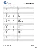
The NX2LP supports industry leading 8-bit NAND Flash inter-

faces and both common NAND page sizes of 512 and 2k

bytes. Eight chip enable pins allow the NX2LP to be connected

to up to eight single- or four dual-device NAND Flash chips.
Certain NX2LP features are configurable, enabling the NX2LP

to meet the needs of different designs’ requirements. 

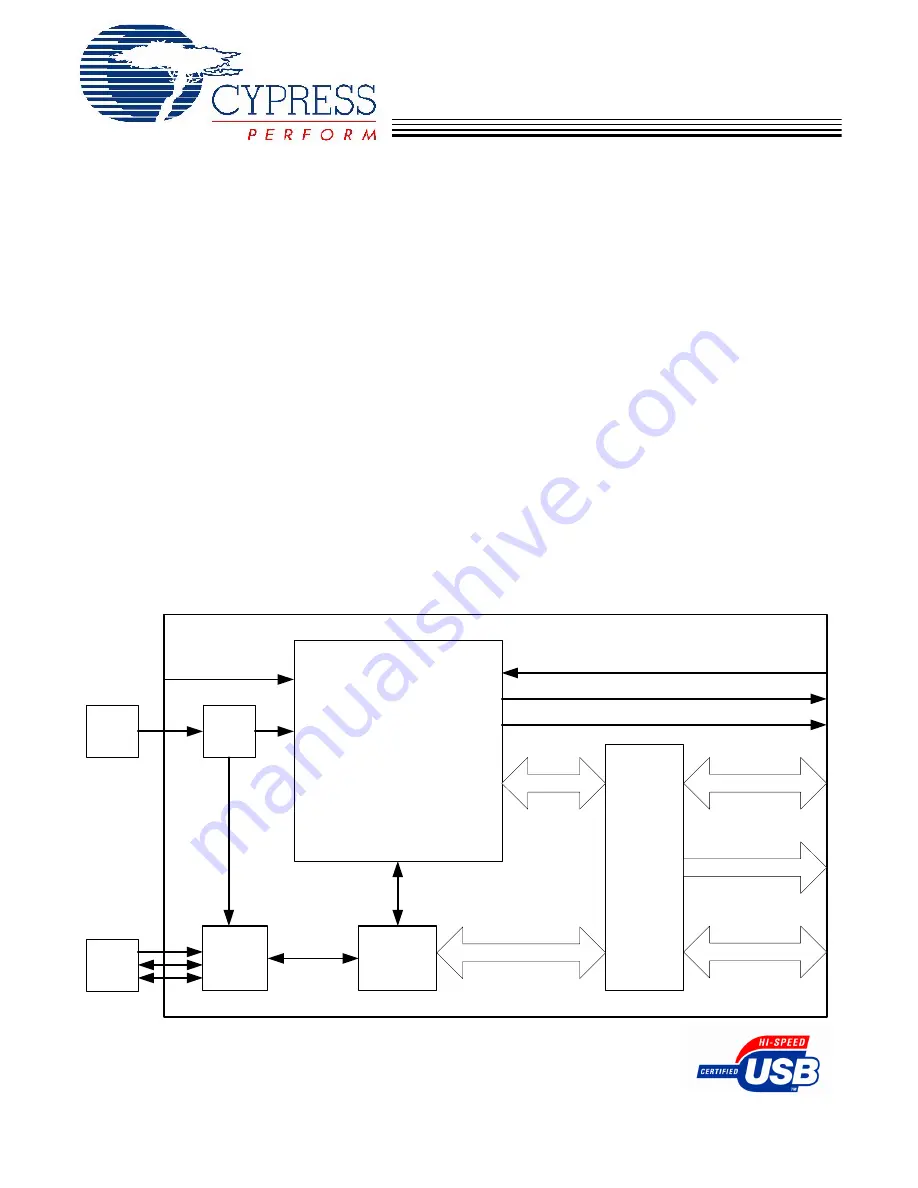
Figure 1-1. NX2LP Block Diagram

USB 2.0

Xceiver

Smart HS/

FS USB

Engine

NAND Flash

Interface

Logic

8-bit Data Bus

NAND Control Signals

EZ-USB NX2LP

Internal Control Logic

PLL

24 MHz

Xtal

VBUS

D+

D-

Data

Control

Chip Reset

LED1#

LED2#

Write Protect

Chip Enable Signals

[+] Feedback 

Summary of Contents for CY7C68023

Page 1: ...6 QFN package 8 mm 8 mm Support for board level manufacturing test via USB interface 3 3V NAND Flash operation NAND Flash power management support 2 0 Introduction The EZ USB NX2LP NX2LP implements a USB 2 0 NAND Flash controller This controller adheres to the Mass Storage Class Bulk Only Transport Specification The USB port of the NX2LP is connected to a host computer directly or via the downstre...

Page 2: ...0 AGND GND GND Ground 11 VCC PWR PWR 3 3V supply 12 GND GND GND Ground 13 N C N A N A No connect 14 GND GND GND Ground 15 Reserved N A N A Must be tied HIGH no pull up resistor required Note 1 A sign after the pin name indicates that it is an active LOW signal RESET GND N C N C WP_SW WP_NF LED2 LED1 ALE CLE VCC RE1 RE0 WE R_B1 R_B2 AVCC XTALOUT XTALIN AGND AVCC DPLUS DMINUS AGND VCC GND N C GND 15...

Page 3: ... Address latch enable 35 LED1 O Z Data activity LED sink 36 LED2 O Z Chip active LED sink 37 WP_NF O Z Write protect NAND Flash 38 WP_SW I Z Write protect switch input 39 N C N A N A No connect 40 N C N A N A No connect 41 GND GND GND Ground 42 RESET I Z NX2LP chip reset 43 VCC PWR PWR 3 3V supply 44 Reserved N A N A Must be tied HIGH 45 CE0 O Z Chip enable 0 46 CE1 O Z Chip enable 1 47 CE2 O Z Ch...

Page 4: ... I O bus is an address The data is latched into the NAND Flash address register on the rising edge of WE when ALE is HIGH 3 3 9 LED1 The Data Activity LED output pin is used to indicate data transfer activity LED1 is asserted LOW at the beginning of a data transfer and set to a high Z state when the transfer is complete If this functionality is not utilized leave LED1 floating 3 3 10 LED2 The Chip...

Page 5: ... the NX2LP behaves as a USB 2 0 Mass Storage Class NAND Flash controller This includes all typical USB device states powered configured etc The USB descriptors are returned according to the data stored in the configuration data memory area Normal read and write access to the NAND Flash is available in this mode 6 2 Manufacturing Mode In Manufacturing mode the NX2LP enumerates using the default des...

Page 6: ...d length of 20 30 mm Maintain a solid ground plane under the DPLUS and DMI NUS traces Do not allow the plane to be split under these traces Place no vias on the DPLUS or DMINUS trace routing Isolate the DPLUS and DMINUS traces from all other signal traces use 10 mm spacing for best signal quality Source for recommendations EZ USB FX2 PCB Design Recommendations www cy press com cfuploads support ap...

Page 7: ...Crystal Input LOW Voltage 0 5 0 8 V VOH Output Voltage High IOUT 4 mA 2 4 V VOL Output Voltage Low IOUT 4 mA 0 4 V IOH Output Current High 4 mA IOL Output Current Low 4 mA CIN Input Pin Capacitance All but D D 10 pF Only D D 15 pF ICC Supply Current USB High Speed 50 mA USB Full Speed 35 mA ISUSP Suspend Current CY7C68023 Connected 0 5 1 2 3 mA Disconnected 0 3 1 0 3 mA CY7C68024 Connected 300 380...

Page 8: ...oducts in life support systems application implies that the manufacturer assumes all risk of such use and in doing so indemnifies Cypress against all charges 14 0 Package Diagram 15 0 Disclaimers Trademarks and Copyrights EZ USB NX2LP is a trademark and EZ USB is a registered trademark of Cypress Semiconductor Corporation All product and company names mentioned in this document are the trademarks ...

Page 9: ...t Number 38 08055 REV ECN NO Issue Date Orig of Change Description of Change 286009 SEE ECN GIR New Data Sheet Preliminary Information A 334796 SEE ECN GIR Adjusted default VID PID released as final B 397024 SEE ECN GIR Changed Vcc to 10 in DC Characteristics table Changed the supply voltage tolerance to 10 in the Operating Conditions section Added new logo Feedback ...

Reviews: