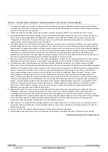
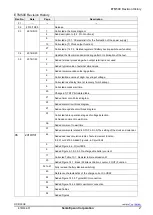
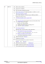
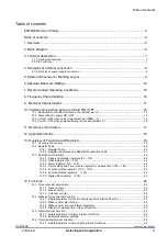
background image


ETM50E Revision History 


Real Time Clock Module 


RX8130CE 


ETM50E-07 


Product name 

Product number 

RX8130CE 

X1B000311000100 

Application manual 

Summary of Contents for RX8130CE

Page 1: ...ETM50E Revision History Real Time Clock Module RX8130CE ETM50E 07 Product name Product number RX8130CE X1B000311000100 Application manual ...

Page 2: ... electronic applications and specifically designated applications Anticipated Purpose Epson products are NOT intended for any use beyond the Anticipated Purpose that requires particular quality or extremely high reliability in order to refrain from causing any malfunction or failure leading to critical harm to life and health serious property damage or severe impact on society including but not li...

Page 3: ...recovery form backup 9 Corrected access wait time 20 Changed 7 TSTP bit related table 21 Added timer circuit block diagram 25 Added alarm circuit block diagram 27 Added time update circuit block diagram 30 Corrected table operation stages of voltage detection 36 Added comment to wait time 36 Added comment to wait time 37 Added comments related to STOP bit in 3 The setting of the clock and calendar...

Page 4: ...n Error tF VDET1 from VDD OFF Correct tF VCLK from VDD OFF 4 Addition that describes the risk of not satisfying tR tF 5 Description of Table11 was updated 21 13 2 2 Register initial value Added description that value are same in after software Reset 39 1 Graph is added for the charge current to Battery Figure27 VBAT charge current characteristics VDD 3 0 V 5 5 V 2 Charging circuit diagram is added...

Page 5: ...nctions 19 13 2 Register Table 20 13 2 1 Register Table 20 13 2 2 Register initial value and Read Write operation Table 21 13 3 Description of registers 22 13 3 1 Clock and calendar registers 0h 16h 22 13 3 2 RAM registers 20h 23h 22 13 3 3 Alarm registers 17h 19h 22 13 3 4 Timer setting and Timer counter register for wakeup timer 1Ah 1Eh 22 13 3 5 Function related register 1 1Ch 1Eh 22 13 3 6 Fun...

Page 6: ... INIEN bit 1 48 15 9 Backup power supply VBAT voltage and a charge state 49 16 Reset output function 50 17 Digital offset function 51 17 1 Digital offset register 51 17 2 Effect of the digital offset function to other functions 52 18 Flow chart 53 18 1 Initializing example 53 18 2 Software Reset 54 18 3 Example of Initialization routine 55 18 4 Example of Initialization routine only clock usage 56...

Page 7: ...etc 1 Overview RX8130CE is a real time clock module of the I2 C serial interface system 32 768 kHz crystal and oscillator is built in it The real time clock function incorporates not only a calendar and clock counter for the year month day day of the week hour minute and second but also a time alarm wakeup timer and time update interruption among other features By the backup battery charge control...

Page 8: ...l after 60ms IRQ Output Interrupt output by Alarm and Timer events N ch open drain This pin can output even a backup mode VDD This is a power supply pin for the internal logic VIO This is an interface power supply pin Connect the same power supply as the MCU VOUT Internal voltage output pin Connect smoothing capacitor of 1 0uF VBAT This is a power supply pin for backup battery This is a pin to con...

Page 9: ...ndary battery EDLC or 0 1 F 1 0 F VOUT 0 1 F Figure 3 Circuit EX1 2 Same I F voltage and charge voltage CHGEN 1 INIEN 1 VDD VBAT VIO 3 0 V 3 0 V R 0 1 F Secondary battery EDLC or 1 0 F VOUT 0 1 F Figure 4 Circuit EX2 3 Primary battery as backup CHGEN 0 VDD VBAT VIO 3 0 V 1 k Max 0 1 F Primary battery 1 0 F VOUT 0 1 F Figure 5 Circuit EX3 4 Case of VDD supply only VDD VBAT VIO 3 0 V 0 1 F 0 1 F 1 0...

Page 10: ... 2 0 2 Typ 3 24 CE PKG Rev 04 2 5 0 2 Typ 2 54 1 0Max 0 7 0 3 0 62 0 42 0 2 Min 0 4 0 35 0 7 0 4 0 9 1 1 0 3 0 7 0 4 0 9 1 1 Type 1 for small mounting area Type 2 Figure 7 External Dimension and Soldering pattern 5 2 Marking Layout RX8130CE 1 Pin Mark Model Production lot R8130 A123B Contents displayed indicate the general markings and display but are not the standards for the fonts sizes and posi...

Page 11: ...ode VDD 1 25 3 0 5 5 V Interface supply voltage VIO INIEN 0 1 6 3 0 5 5 V INIEN 1 VDET1 3 0 5 5 V Clock supply voltage VCLK Backup operation mode VOUT 1 1 3 0 5 5 V Operating temperature T use No condensation 40 25 85 C Minimum clock supply voltage of VCLK is available after initializing in VDD VDET11 8 Frequency Characteristics Table 4 Frequency Characteristics Unless otherwise specified GND 0 V ...

Page 12: ...eset releases 2 67 2 75 2 83 V Detector Threshold Voltage2 falling edge of VDD VDET12 2 7 V setting Reset output 2 62 2 70 2 78 V Detector Threshold Voltage3 rising edge of VDD VDET2 Switching voltage from VBAT to VDD 1 25 1 35 1 45 V Detector Threshold Voltage3 falling edge of VDD VDET2 Switching voltage from VDD to VBAT 1 20 1 30 1 40 V Detector Threshold Voltage1 rising edge of VBAT VDET31 Char...

Page 13: ...t voltage 1 VVOUT1 VDD 3 0 V IOUT 1 mA VDD 0 06 V VOUT output voltage 2 VVOUT2 VBAT 3 0 V IOUT 0 1 mA VBAT 0 02 V High level input voltage VIH1 SCL SDA 0 8 VIO 5 5 V Low level input voltage VIL SCL SDA GND 0 3 0 2 VIO V High level output voltage VOH FOUT IOH 1 mA VIO 0 5 VIO V Low level output voltage VOL1 FOUT IOL 1 mA GND GND 0 5 V VOL2 RST IRQ VIO 5 V IOL 1 mA GND GND 0 2 5 V VOL3 VIO 3 V IOL 1...

Page 14: ...SDA SCL START CONDITION S BIT 7 MSB A7 BIT 6 A6 ACK A Protocol tBUF tSU STO STOP CONDITION P START CONDITION S P A tHD STA tSU STA S BIT 0 LSB R W S tSP Figure 9 I2 C Bus Interface Timing Chart Warning When accessing this device all communication from transmitting the start condition to transmitting the stop condition after access should be completed within 0 95 seconds If such communication requi...

Page 15: ...LAY VDET11 VDET12 t_str tDELAYF t_str is oscillation startup time See Table4 Figure 10 Reset signal timing chart Power Initial Supply Table 10 Reset timing Item symbol Min Typ Max unit Voltage detection time to reset release t_int 35 ms Reset delay time Recovery from Backup t_int t_DELAY tDELAY_B 60 95 ms VDD RST tDELAY VDET11 or VDET12 t_Init tDELAY_B VDET2 t_int is an intermittence drive timing ...

Page 16: ...y software See 18 2 Software Reset 3 When fluctuation of VDD is out of specifications tF or tR2 it may be occur the followings a momentary stop of crystal oscillation a set of VLF by VOUT voltage drop lower than VCLK and so on 4 The timing at which the I2 C Bus interface is enabled differs in when the initial power of VDD is turned on and when VDD is turned on from backup mode See the tCL and tCU ...

Page 17: ...ET11 to Access start 30 ms Access suspended time tCD The time from the end of I2 C access to the disable of I2 C 0 ms Power supply fall time tF From VDD to VDD VCLK 1 ms V Power supply rise time tR2 Time to restore VDD to operating voltage 1 ms V Access wait time tCU VDD VDET1x to Access start 35 ms tR1 tR2 and tF specify that there is no voltage fluctuation faster slower than the Min Max specific...

Page 18: ...Frequency deviation in any temperature 1 C2 Coefficient of secondary temperature 0 035 0 005 10 6 C2 T C Ultimate temperature 25 5 C X C Any temperature 2 To determine overall clock accuracy add the frequency precision and voltage characteristics f f f fo fT fV f f Clock accuracy stable frequency in any temperature and voltage f fo Frequency precision fT Frequency deviation in any temperature fV F...

Page 19: ...t terminal is open state it causes increase of a consumption electric current and the behavior that are instability Please fix an unused input terminal to the voltage that is near to VIO or GND 2 Notes on packaging 1 Soldering heat resistance If the temperature within the package exceeds 260 C the characteristics of the crystal oscillator will be degraded and it may be damaged The reflow condition...

Page 20: ...n measures the operation time on the main power supply and the operation time on the backup power supply and can automatically sum them up 4 Alarm interrupt function The alarm interrupt function generates interrupt events for alarm settings such as date day hour and minute settings When an interrupt event occurs the AF bit value is set to 1 and the IRQ pin goes to low level to indicate that an eve...

Page 21: ...bit 0 20 23 RAM User Register 32 bits 4 word x 8 bit Address h Function bit 7 bit 6 bit 5 bit 4 bit 3 bit 2 bit 1 bit 0 30 Digital offset DTE L7 L6 L5 L4 L3 L2 L1 31 Extension Register1 VBLFE After the initial power up from 0 V or in case the VLF bit returns 1 make sure to initialize all registers before using the RTC Be sure to avoid entering incorrect date and time data as clock operations are n...

Page 22: ...EC 0 X X X X X X X 11 MIN 0 X X X X X X X 12 HOUR 0 0 X X X X X X 13 WEEK 0 X X X X X X X 14 DAY 0 0 X X X X X X 15 MONTH 0 0 0 X X X X X 16 YEAR X X X X X X X X 17 MIN Alarm X X X X X X X X 18 HOUR Alarm X X X X X X X X 19 WEEK Alarm X X X X X X X X DAY Alarm X X X X X X X 1A Timer Counter 0 X X X X X X X X 1B Timer Counter 1 X X X X X X X X 1C Extension Register 0 0 0 0 0 1 0 0 1D Flag Register ...

Page 23: ...mer interrupt function is not being used the wakeup timer control register can be used as a RAM register In such cases stop the wakeup timer function by writing 0 to the TE and TIE bits See 14 2 Wakeup Timer Interrupt Function for the details 13 3 5 Function related register 1 1Ch 1Eh 1 FSEL1 FSEL0 bit A combination of the FSEL1 and FSEL0 bits are used to select the frequency to be output The choi...

Page 24: ...UT functions When STOP 1 32 768 kHz and 1024 Hz output is possible But 1 Hz output is disabled 4 Switchover function cannot work in order that the VDD voltage drop detection stops even if a main power supply falls 8 RSF bit This flag bit holds the result of detecting the reset voltage 13 3 6 Function related register 2 1Fh 1 SMPTSEL1 SMPTSEL0 bit Operation time setting of a voltage detector circui...

Page 25: ...1 MIN 0 0 1 1 1 0 0 1 12 HOUR 0 0 0 1 0 1 1 1 13 WEEK 0 0 0 0 0 0 0 1 14 DAY 0 0 1 0 1 0 0 1 15 MONTH 0 0 0 0 0 0 1 0 16 YEAR 1 0 0 0 1 0 0 0 Note with caution that writing non existent time data may interfere with normal operation of the clock counter 14 1 1 Clock counter 1 SEC MIN register These registers are 60 base BCD counters These registers are incremented at the timing when carry is genera...

Page 26: ...rsday 0 0 0 1 0 0 0 0 10 h Friday 0 0 1 0 0 0 0 0 20 h Saturday 0 1 0 0 0 0 0 0 40 h Do not set 1 to more than one day at the same time 14 1 3 Calendar counter 1 DAY MONTH register The DAY register is a variable between 28 base and 31 base BCD counter that is influenced by the month and the leap year The MONTH register is a 12 base BCD counter triggered by carryover of the day register 2 YEAR regi...

Page 27: ...r Timer Counter 1 0 This register is used to set the default preset value for the counter Any count value from 1 0001 h to 65535 FFFFh can be set Be sure to write 0 to the TE bit before writing the preset value When TE 0 read out data of timer counter is default Preset value And when TE 1 read out data of timer counter is just counting value But when access to timer counter data counting value is ...

Page 28: ...E TBKON bit Note The resolution of the count value depends on the source clock Figure 18 Wakeup timer block diagram 3 TE bit Timer Enable When TE bit is 0 the default preset can be checked by reading this register Table 17 Wakeup timer control TE Data Description Write 0 Stops wakeup timer interrupt function Clearing this bit to zero does not enable the IRQ low output status to be cleared to Hi z ...

Page 29: ...s from low to Hi z 1 When a wakeup timer interrupt event occurs an interrupt signal is generated IRQ status changes from Hi z to low 6 TBKON TBKE bit This function selects the operation time with the main power supply or the operation time with the backup power supply The count value is added Table 20 Wakeup timer normal mode backup mode control operation TBKE TBKON Description Write 0 X This sett...

Page 30: ...mer start timing Counting down of the wakeup timer value starts at the rising edge of the SCL ACK output signal that occurs when the TE value is changed from 0 to 1 TSEL0 TE TSEL2 1 TSEL1 Count down IRQ pin SDA Master SCL Internal timer WADA A SDA Slave ACK Figure 19 Wakeup timer start sequence ...

Page 31: ... 0 0 0 64 Hz TSEL2 0 TSEL1 0 0 1 1 Hz TSEL2 0 TSEL1 0 1 0 1 60 Hz TSEL2 0 TSEL1 0 1 1 1 3600 Hz TSEL2 1 TSEL1 0 0 0 0 1 244 14 s 15 625 ms 1 s 1 min 1 h 410 100 10 ms 6 406 s 410 s 410 min 410 h 3840 0 9375 s 60 000 s 3840 s 3840 min 3840 h 4096 1 0000 s 64 000 s 4096 s 4096 min 4096 h 65535 15 9998 s 1023 984 s 65535 s 65535 mi n 65535 h 14 2 4 Diagram of wakeup timer interrupt function Figure 20...

Page 32: ...ime that must be matched 2 When a time update interrupt event occurs the UF bit value becomes 1 3 When the UF bit value is 1 its value is retained until it is cleared to zero 4 When a time update interrupt occurs IRQ pin output is low if UIE 1 If UIE 0 when a timer update interrupt occurs the IRQ pin status remains Hi Z 5 Each time an event occurs IRQ pin output is low only up to the tRTN time whi...

Page 33: ...it The minute hour day and date when an alarm interrupt event will occur is set using this register and the WADA bit In the WEEK alarm Day alarm register Reg 19h the setting selected via the WADA bit determines whether WEEK alarm data or DAY alarm data will be set If WEEK has been selected via the WADA bit multiple days can be set such as Monday Wednesday Friday Saturday When the settings made in ...

Page 34: ... interrupt event has occurred Table 25 Alarm Interrupt control The AIE bit is only output control of the IRQ terminal It is necessary to clear an AF flag to cancel alarm 14 3 2 Examples of alarm settings 1 Example of alarm settings when Week has been specified and WADA bit 0 Table 26 WEEK alarm example Week is specified WADA bit 0 Week Alarm HOUR Alarm MIN Alarm bit 7 AE bit 6 S bit 5 F bit 4 T bi...

Page 35: ...d 0 0 0 0 0 0 0 1 07 h AE bit 1 15th of each month for 30 minutes each hour Hour value is ignored 0 0 0 1 0 1 0 1 AE bit 1 30 h Every day at 6 59 PM 1 18 h 59 h Don t care 14 3 3 Diagram of alarm interrupt function Figure 22 Alarm interrupt inner block diagram AIE bit IRQ output AF bit Event occurs 1 0 Hi z L 1 0 Internal operation Write operation Figure 23 Alarm Interrupt time chart Internal minu...

Page 36: ...ate interrupt events Table 28 Second Minute selection 2 UF bit Update Flag This flag bit value changes from 0 to 1 when a time update interrupt event occurs Table 29 Time update Flag UF Data Description Write 0 Clearing this bit to zero enables IRQ low output to be canceled IRQ remains Hi z when a time update interrupt event has occurred 1 Invalid writing a 1 will be ignored Read 0 1 Time update i...

Page 37: ...upt function diagram Figure 24 Time update inner block diagram Figure 25 Time update time chart UIE bit IRQ output UF bit Carry tRTN period period period period 1 0 Hi z L 1 0 Internal operation Write operation Carry Sec 64 Hz Update Control Circuit USEL bit UF 0 Clear Carry Min tRTN UF Flag UIE bit IRQ ...

Page 38: ...eared to 0 and waiting for next low voltage detection 1 Invalid writing 1 will be ignored Read 0 Oscillation status is normal RTC register data are valid 1 Oscillation stop is detected RTC register data are invalid Should be initialized of all register data VLF is maintained till it is cleared by zero 14 6 FOUT function The clock signal can be output via the FOUT pin Output is stopped upon detecti...

Page 39: ...sult of the supply voltage detection of VDET2 and the RTC changes the operating modes between normal mode RTC power supply VDD or backup mode RTC power supply VBAT The RTCs backup function is built in a way to prevent reverse current flow from VBAT to VDD While in backup mode the I2C bus and FOUT function are switched off and related terminals switched to Hi Z Figure 26 Battery backup switchover b...

Page 40: ...hen VDD voltage is high The charge current increase And when little voltage differences of VDD and VBAT charge current is decreasing A vertical axis shows charge current Ichg and a horizontal axis shows voltage difference Vdef between VDD and VBAT VDD 3 0 V VDD 5 5 V Figure 27 VBAT charge current characteristics VDD 3 0 V 5 5 V 15 4 Re Chargeable battery Voltage Current features Figure 28 Re charg...

Page 41: ...IEN bit Note1 When INIEN is used with 0 it must be set up INIEN 1 before the setting once at least When INIEN bit is used with 0 from just Power On Reset value all the time there is the case that INIEN 0 mode is incorrect working For example Power switching doesn t work Therefore that an INIEN bit is set to 1 in initial setting is recommended See initial setting example Note2 when INIEN set to 1 f...

Page 42: ...15 Battery backup switchover function RX8130CE Jump to Top Bottom ETM50E 07 Seiko Epson Corporation 41 Figure 31 Re chargeable battery SW1 SW2 control INIEN 1 CHGEN 1 ...

Page 43: ...15 Battery backup switchover function RX8130CE Jump to Top Bottom ETM50E 07 Seiko Epson Corporation 42 Figure 32 Battery backup SW1 SW2 automatic control ...

Page 44: ... SMPTSEL0 See Figure 31 for VDET3 VDET4 voltage detection timing In case of CHGEN 0 There is no charge operation SW2 OFF Table 36 Voltage detection timing Power supply mode Normal mode Backup battery is charging Normal mode Backup battery is fully charged Normal mode After return from backup VDET1 VDD VDET2 Backup mode Reset detection VDD VDET1 Constantly ON Constantly ON Constantly ON Constantly ...

Page 45: ...ther hand in order to detect a slower external voltage drop on VDD a longer SW1 OFF detection time is needed But longer SW1 OFF period increases the current consumption Users are requested to evaluate SW1 OFF period based on actual system configuration and characteristics In backup mode VDD detection VDET2 is activated once every 31 25 ms Note Re chargeable battery is charged through diode during1...

Page 46: ... 8V 2 75V RSVSEL 0 default VDET12 VDET12 2 7V 2 65V RSVSEL 1 VDET2 Backup switchover recover voltage VDET2 VDET2 1 35V 1 30V VDET3 Full charge detection voltage VDET31 VDET31 3 02V 2 97V BFVSEL 00b default VDET30 VDET30 2 92V 2 87V BFVSEL 01b VDET32 VDET32 3 08V 3 03V BFVSEL 10b VDET4 VBAT low voltage detection voltage VDET4 2 4V 4 The full charge detection VDET3 and low VBAT detection VDET4 contr...

Page 47: ...tion Every 1 s Table 42 VBLFE VBLFE Data Description Write 0 CHGEN 0 VBLF detection not available CHGEN 1 VBLF detection available during normal mode re chargeable battery charging 1 During VDD supply VBLF detection available To use VBLF detection it must be set up INIEN 1 before the setting once at least and VBLFE bit setting During normal mode VDD drive VBAT low voltage Non rechargeable recharge...

Page 48: ...on Corporation 47 15 7 Power supply control By setting battery backup registers INIEN CHGEN the RX8130CE operates like following either in re chargeable battery or non re chargeable battery operation Figure 35 Re chargeable battery operation Figure 36 Non re chargeable battery operation ...

Page 49: ...ge stop VDET 11 VDET 12 2 In case of a voltage rise I2 C FOUT is available I2 C FOUT is disabled 3 3V A function of I2 C and FOUT stops in sync with the RST output 3 3V VDET 11 RST Charge stop VDET 12 VDET 2 VDD Default I2 C FOUT is available I2 C FOUT is disabled Charge enable VDET 3 VBAT 1 and VDD VBAT VDET 11 or VDET 12 Register setting When full charge detection was deactivated VDET3 by regist...

Page 50: ...tage drop VDD VDET2 VBAT low voltage flag VBLF VDET 4 1 In case of voltage rise VDD VDET 2 Charge is enable VDET 3 VBAT and VDD VBAT VDET 3 Charge stop VBAT SW2 OFF 0 1 3 1 V Adjustment by register setting is possible Recharge VDET 3 VBAT Register settings allow to stop or prevent charging or keep charging VBAT as well above upper limit VDET 3 Adjustment by register setting is possible Charge stop...

Page 51: ...reset output function Address h Function bit 7 bit 6 bit 5 bit 4 bit 3 bit 2 bit 1 bit 0 1D Flag Register VBLF 0 UF TF AF RSF VLF VBFF 1F Control Register1 SMP TSEL1 SMP TSEL0 CHG EN INIEN 0 RS VSEL BF VSEL1 BF VSEL0 1 RSVSEL bit Setting of VDET1 voltage level In case VDD drops below this level the RST signal is output and the I F and FOUT output are stopped depending on INIEN bit setting Table 43...

Page 52: ...g a 32 768 kHz signal on FOUT pin this function has no influence since the oscillation frequency of the built in crystal does not change by using this function In case of outputting a 1 Hz or 1024 Hz signal on FOUT the offset correction will cause a certain jitter on the clock signal Alarm function as well as the Wakeup Timer function if source clock lower than 4096 Hz is selected are affected by ...

Page 53: ...ve offset L 7 1 11 57 3 05 4 Dec However decimals are discarded 0000100 bin is set Negative offset L 7 1 128 11 57 3 05 124 Dec However decimals are discarded 1111100 bin is set 17 2 Effect of the digital offset function to other functions Because this function adjusts an internal sub second clock this function affects the a Wakeup timer interrupt function and FOUT function 1 FOUT function 1 Hz se...

Page 54: ...wait time is needed So that it is stable RTC 40 ms is not oscillation startup time When the power supply conditions for which Power On Reset is executed cannot be satisfied then must be execute a Dummy read Dummy read is one time read access to a free address Ignore ACK NACK from RX8130CE in Dummy read Judge RX8130CE returned from backup normally or fail When the power conditions for which the pow...

Page 55: ...s performed by this processing As for the register value after software reset See 13 2 2 Register initial value Notes It has possibility leak current occurs from step 6 to step 10 because all power switch are turned to ON while this After step 5 please complete the process immediately 3 In a dummy lead ignore NACK ACK from RTC 10 TEST bit is cleared automatically in step10 Both time and a calendar...

Page 56: ...tion When the alarm interrupt function is not being used the Alarm registers can be used as a RAM register In such cases be sure to write 0 to the AIE bit Interval timer function Configure the interval timer function When the interval Timer function is not being used the Timer Counter register can be used as a RAM register In such cases stop the interval timer function by writing 0 to the TE and T...

Page 57: ...Write information of year month date day of the week hour minute second which is necessary to set or reset In case of initialization please initialize all data STOP 0 Write 0 to STOP bit for restart clock updating Clock is started at the time It is able to set time even if not combined use of STOP bit Please note that clock is started at the time of writing second in case STOP bit is not used Whil...

Page 58: ... the wakeup timer interrupt function Next process Reg 1Ah 1Bh Set initial value of down counter Start count Set TE bit to 1 to start timer interrupt function When start timers interrupt function please surely set reset implement 2 initial value of down counter in advance Reg 1Eh Select and set IRQ output Select a power supply condition of a count 1 Countdown is suspended with TSTP 0 1 and countdow...

Page 59: ...mple of the Alarm interrupt function Next process Reg 1Eh Select and set IRQ1 output in AIE bit Reg 1Ch Select week or day in WADA bit Reg 1Dh Clear AF bit Alarm setting Set AIE bit to 0 to stop Alarm interrupt function Set alarm data Reg 1Eh Reg 17h 19h Figure 46 Example flow Alarm interruption ...

Page 60: ... condition This condition regulates how communications on the I2 C Bus are terminated The SDA level changes from low to high while SCL is at high level 3 Repeated START condition RESTART condition In some cases the START condition occurs between a previous START condition and the next STOP condition in which case the second START condition is distinguished as a RESTART condition Since the required...

Page 61: ...eceiver Other I2 C Bus device CPU etc RX8130CE SDA SCL VIO Master Transmitter Receiver Slave Transmitter Receiver Figure 48 I2C Bus connection Any device that controls the data transmission and data reception is defined as a Master and any device that is controlled by a master device is defined as a Slave The device transmitting data is defined as a Transmitter and the device receiving data is def...

Page 62: ...signal from RX8130CE 8 Repeat 6 and 7 if necessary Addresses are automatically incremented 9 CPU transfers stop condition P S 1 0 R W 0 3 Address 4 0 5 0 Data 8 P 9 ACK signal from8130CE Data 6 0 7 2 Slave address 2 Address specification read sequence After using write mode to write the address to be read set read mode to read the actual data 1 CPU transfers start condition S 2 CPU transmits the R...

Page 63: ... such cases the address for each read operation is the previously accessed address 1 1 CPU transfers start condition S 2 CPU transmits the RX8130CE s slave address with the R W bit set to read mode 3 Check for ACK signal from RX8130CE from this point on the CPU is the receiver and the RX8130CE is the transmitter 4 Data is output from the RX8130 to the address following the end of the previously ac...

Page 64: ...20 Circuit Diagram connection RX8130CE Jump to Top Bottom ETM50E 07 Seiko Epson Corporation 63 20 Circuit Diagram connection 20 1 Typical MCU connection Figure 49 Typical MCU connection ...

Page 65: ...uit Diagram connection RX8130CE Jump to Top Bottom ETM50E 07 Seiko Epson Corporation 64 20 2 32 768 kHz oscillator application connection See also 14 6 FOUT function Figure 50 32 768 kHz oscillator connection ...

Page 66: ...urce clock selection 26 Table 17 Wakeup timer control 27 Table 18 Wakeup timer interrupt detection flag 28 Table 19 Wakeup timer interrupt control 28 Table 20 Wakeup timer normal mode backup mode control 28 Table 21 Wakeup timer stop control 28 Table 22 Wakeup timer interrupt cycles 30 Table 23 WEEK DAY control 33 Table 24 Alarm Flag 33 Table 25 Alarm Interrupt control 33 Table 26 WEEK alarm examp...

Page 67: ...ncy temperature characteristics 17 Figure 16 Basic 32 768 k Hz oscillation counter FOUT Function 24 Figure 17 Wakeup timer initial sequence 27 Figure 18 Wakeup timer block diagram 27 Figure 19 Wakeup timer start sequence 29 Figure 20 Wakeup timer inner block diagram 30 Figure 21 Wakeup timer timing chart 31 Figure 22 Alarm interrupt inner block diagram 34 Figure 23 Alarm Interrupt time chart 34 Fi...

Page 68: ...peration during voltage rise and down 49 Figure 39 Example flow Power initialization 53 Figure 40 Example Flow Software Reset 54 Figure 41 Example flow Initialization 55 Figure 42 Example flow initialization only clock usage 56 Figure 43 Example flow Clock calendar setting 56 Figure 44 Example flow Clock calendar reading 57 Figure 45 Example flow Wakeup timer interruption 57 Figure 46 Example flow...

Page 69: ...ranch High Tech Building 900 Yishan Road Shanghai 200233 China Shenzhen Branch Room 804 805 8F Tower 2 Ali Center No 3332 Keyuan South Road Shenzhen Bay Nanshan District Shenzhen 518054 China Epson Hong Kong Ltd Unit 715 723 7 F Trade Square 681 Cheung Sha Wan Road Kowloon Hong Kong www epson com hk Epson Taiwan Technology Trading Ltd 15F No 100 Songren Rd Sinyi Dist Taipei City 11073 Taiwan www e...

Reviews: