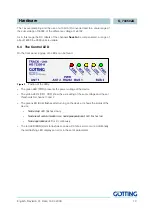
background image

Device Description

G_73350ZA


Interpreter For Inductive 

Guidance Of Vehicles

— CAN-OPEN —

G_73350ZA

English, Revision 01

Dev. by:

W.M.

Date: 14.04.2009

Authors.:

RAD / L.S.

Götting KG, Celler Str. 5, D-31275 Lehrte - Röddensen (Germany), Tel.: +49 (0) 51 36 / 80 96 -0,


Fax: +49 (0) 51 36 / 80 96 -80, eMail: techdoc@goetting.de, Internet: www.goetting.de

Summary of Contents for HG 73350ZA

Page 1: ...Guidance Of Vehicles CAN OPEN G_73350ZA English Revision 01 Dev by W M Date 14 04 2009 Authors RAD L S Götting KG Celler Str 5 D 31275 Lehrte Röddensen Germany Tel 49 0 51 36 80 96 0 Fax 49 0 51 36 80 96 80 eMail techdoc goetting de Internet www goetting de ...

Page 2: ...0 6 Software 11 6 1 Monitor program 11 6 1 1 Main menu 11 6 1 2 Antenna menu 12 6 1 3 CAN menu 14 6 2 Changing the surrounding 16 6 3 Updating the software 16 7 CAN Interface 18 7 1 Description of the process data objects PDOs 18 7 1 1 Transmission objects 18 7 1 2 Receiving objects 19 7 2 Heartbeat 20 7 3 Writing on service data objects SDOs 20 7 4 Object directory 21 7 4 1 Communication specific...

Page 3: ..._1 29 7 4 4 16 Mapping TxPDO_2 30 7 4 4 17 Manufacture Parameter parameters of the antenna 31 7 4 4 18 Manufacture parameter calibration of the antenna 32 7 4 4 19 Manufacture parameter node parameter 33 7 4 4 20 8 Bit Digital Input transmitted in TxPDO 1 34 7 4 4 21 16 Bit Analog Inputs transmitted in TxPDO 1 und TxPDO 2 34 8 Troubleshooting 35 9 Technical data 36 10 Appendix 37 A Block diagram 3...

Page 4: ...through out the entire document In addition each document has an index listed behind the front page including pages and whenever the document has more than 10 pages following the actual system description a figure and table index in the back In certain cases for long and or complicated documents a subject index is added Each document provides a table block with metainformation on the front page in...

Page 5: ...ile DS 401 is implemented The parametrization can be carried out by a terminal programm e g Hyperterm us ing the serial interface or the SDOs of the CAN open protocol This documentation was written for hardware version 73350ZA2 and software version 73350A01 14 or higher Components At the time this manual was printed the interpreter can be combined with the following antennas G 19200ZC G 19200YC G ...

Page 6: ... The two panel jacks are shown in Figure 1 named ANT1 and ANT2 They are allocated as follows It does not matter whether one or two antennas are connected When using only one antenna ANT1 or ANT2 can be chosen The displaying of CD1 CD2 on the front panel see Postion of the LEDs on page 10 refers to the corresponding antenna input The input voltage of ANT1 and ANT2 are processed internally as US1 UD...

Page 7: ... different manufacturers and are availbale for most plugs and jacks The CAN connecters can also be used as power supply ATTENTION Do not connect 24V to pin 4 or 5 3 2 3 Power supply and serial interface Here a 5 pin M12 panel plug is used in the figure Casing antenna HG 73350 on page 6 this plug called PWR RS232 has the following pin allocation This connection serves the power supply Additionally ...

Page 8: ...eter is able to calculate and display the deviation in mm For a position calibration the following things are required correct positioning of the antenna I e its position has to be the same as the one set in the interpreter see also 6 1 2 on page 12 and 7 4 4 17 on page 31 a guide wire with a rated current if possible 10 kHz The calibration can be started by using the CAN bus or the serial interfa...

Page 9: ...ave been scaled an incoming amplitude of 1 VPP controls the the sum channel and the difference channel An input amplitude of 1 Vss reaches a full range of 75 between sum channel and the difference channel The CAN baudrate is preset to 125 kbaud the node ID to 1 The maximal incoming signal of all data streams having other frequencies is 5 VPP As the parameters of the device reading height wire curr...

Page 10: ...Ds can be found Figure 2 Postion of the LEDs The green LED PWR presents the power voltage of the device The yellow LEDs CD1 CD2 show the exceeding of the sum voltage and the set thresholds for channel 1 and 2 The green LED BUS flashes after turning on the device It shows the status of the device Node stop LED flashes slowly Node reset communication and node preoperational LED flashes fast Node ope...

Page 11: ...m voltage is maximal 16 x 1024 16384 and for the difference voltage 16 x 512 until 16 x 511 8192 until 8176 X1 X2 X1 and X2 present the calculated values for the collateral deviation of the antennas above the guide wire in a range from 255 to 255 in mm The value of the threshold will be 256 if the corresponding voltages of S1 respectively S2 fall below the set threshold Status The hexadecimal outp...

Page 12: ...he device here threshold 2 exceeded then Us1 0 and Ud1 17 followed by Us2 9626 and Ud2 3333 The last displayed numbers show the collateral deviations for antenna 1 and antenna 2 If no wire was detected 256 is displayed as distance value By using the protocol function of Hyperterm the data can be logged A stops the out put with U the firmware can be updated the Servicemenu cannot be modified by the...

Page 13: ...f the sensor can be modified With I the internal height which is specified for each type of antenna can be entered NOTE The sum of the values entered under H and I are used to cal culate the distance C starts the calibration of the distance output Now the corresponding antenna has to be moved in an area of 2x height over the guide wire For the calibration a 10 kHz wire frequency is recommended as ...

Page 14: ...e maxima and the reading heigt which was entered in the antenna menu To save this values permanent ly L has to be pressed in the main menu 6 1 3 CAN menu The CAN menu is made up as follows Figure 6 Screenshot CAN menu S1 3780 D1 3617 S2 3133 D2 4590 X1 62 X2 99 Status 0xc0 Us1 3795 Udl1 0 Udr1 3645 shift Antenna 1 from 2 H to 2 H and press any key when ready S1 0 D1 6 S2 0 D2 40 X1 256 X2 256 Stat...

Page 15: ...transmission If both values are 0 PDO_1 will no be transmitted by pressing F the operational mode PDO_2 is selected Choosing a value between 1 and 240 the synchronous cyclical mode can be chosen By selecting 255 the asynchronous mode is set The two following modes are only available in the asynchronous mode G is the inhibit time of PDO_2 In PDO_2 the four analog antenna voltages are transmitted Th...

Page 16: ...ound above the conductor By using the cor responding potentiometer for the antenna it has to be reduced to 12000 units The maximum of the difference voltage can be found at a corresponding distance col lateral from the conductor By using the corresponding potentiometer for the antenna it has to be reduced to 6000 units 6 3 Updating the software The used processor AT89C51CC03 can be programmed with...

Page 17: ...programmation is displayed by The symbol o shows that the procedure is fin ished Figure 8 Screenshot firmware upload Afterwards the new firmware is started immediately If the transmission was not suc cessful neither the old nor the new firmware can be found in the device Yet the flash loader is always available and starts automatically after rebooting the device Please wait for R and transfer Inte...

Page 18: ...g the non cyclical transmission asynchronous mode the inhibit time in the CAN menu can be adjusted using the se rial monitor see 6 1 3 on page 14 This is important as the the constant changes may affect the BUS A PDO can be transmitted cyclical anyway The corresponding event time is to choose and the inhibit time has to be set to 0 A TxPDO can be activated permanently by choosing the asynchonous m...

Page 19: ...ontains 4 bytes for the frequencies F1 and F2 in Hz The order of the bytes within the 16bit words can be al tered using the CAN menu L see 6 1 3 on page 14 or the SDO with index 0x2003 02 Node config Bit no Value Meaning 7 0x80 Us1 exceeded chosen threshold for channel 1 6 0x40 Us2 exceeded chosen threshold for channel 2 5 0x20 Toggle Bit changes its status after each transmission of PDO_1 4 0x10 ...

Page 20: ...mation i e each incoming message is confirmed The identifiers for read and write access are Read access 0x600 Node Adresse Write accessf 0x580 Node Adresse The SDO telegramms are written according to CiA standard DS 301 The error codes which may occur due to an erroneous communication are listed in the following table Value Number Value range Annotation F1 Unsigne d 16 1000 28000 frequency of wire...

Page 21: ...or save has not been used When calling calibration signature cali has not been used SDO_ABORT_PARA_VALUE 0x06090030 parameter value range exceeded SDO_ABORT_PARA_TO_HIGH 0x06090031 parameter value too high Communication specific entries located from 0x1000 to 0x1FFF Index Subindex Access Content EEProm 0x1000 0 RO Device Typ 0x1001 0 RO Error Register 0x1005 0 RO COB ID Sync Message 0x1008 0 RO Nu...

Page 22: ...eive PDO_1 1 RW COB ID 2 RO Transmission Type 0x1600 0 RO Number of Objects mapped to Receive PDO_1 1 RO Specification of Appl Object 1 2 RO Specification of Appl Object 2 0x1800 0 RO Number of entries of Transmit PDO_1 1 RW COB ID 2 RW Transmission Type C 3 RW Inhibit Time C 5 RW Event Time C 0x1801 0 RO Number of entries of Transmit PDO_2 1 RW COB ID 2 RW Transmission Type C 3 RW Inhibit Time C ...

Page 23: ...s höchste Bit verändert werden um den PDO vorübergehend zu de aktivieren Manufacturer entries from 0x2000 on Index Subindex Access Content EEProm 0x2000 0 RO Number of Parameter 1 RW Frequency 1 M 2 RW Frequency 2 M 3 RW Threshold CD1 LED M 4 RW Threshold CD2 LED M 5 RW Height of Ant 1 M 6 RW Height of Ant 2 M 7 RW Internal Height of Ant 1 M 8 RW Internal Height of Ant 2 M Table 12 CAN overview of...

Page 24: ...2 calibration 0x2002 0 RO Number of Parameter 1 RW Node Baudrate C 2 RW Node ID C 3 RW Node Config C Standard device profile from 0x6000 on Index Subindex Access Content 0x6000 0 RO Number of 8 Bit Digital Inputs 1 RO Systemstatus 0x6401 0 RO Number of 16 Bit analog Inputs 1 RO Analog Input Us1 2 RO Analog Input Ud1 3 RO Analog Input Us2 4 RO Analog Input Ud2 5 RO X1 mm 6 RO X2 mm Table 13 CAN ove...

Page 25: ... Device Type Index Sub Index Name Typ Attr Map Default Meaning 0x1001 00 Error Regis ter Unsigned 8 RO No 0x00 Error register Table 15 CAN Error Register Index Sub Index Name Typ Attr Map Default Meaning 0x1005 00 COB ID SYNC Unsigned 32 RO No 0x80000080 Sync Consumer Sync ID 0x80 Table 16 CAN COB ID SYNC message Index Subindex Name Typ Attr Map Default Meaning 0x1008 00 Device Name Unsigned 8 RO ...

Page 26: ...le 18 CAN Hardware Version Index Subindex Name Typ Attr Map Default Meaning 0x100A 00 Software Version Vis String RO NO 1 14 version der firm ware Table 19 CAN Software Version Index Sub Index Name Typ Attr Map Default Meaning 0x1010 00 Save Parameter Unsigned 8 RO No 0x01 number of sub indexes 01 Save All Unsigned 32 RW No 0x00000001 Save All is possi ble Table 20 CAN Save Parameter Index Sub Ind...

Page 27: ...ucer Heartbeat Time Index Sub Index Name Typ Attr Map Default Meaning 0x1018 00 Identity Object Unsigned 8 RO No 0x03 number of sub indexes 01 Vendor ID Unsigned 32 RO No 0x00000202 manufacturer number deter mined by CiA 02 Product Code Unsigned 32 RO No 0x00073350 name of the device 03 Revision Unsigned 32 RO No 0x00000001 revision of the device 04 Serial Num ber Unsigned 32 RO No 73 7 digit seri...

Page 28: ...gned 32 RO NO 0x20000210 Mapped on Index 0x2000 02 with 16 Bit length Fre quency 2 Table 25 CAN Mapping RPDO_1 Index Sub Index Name Typ Attr Map Default Meaning 0x1800 00 TxPDO_1 Parameter Unsigned 8 RO No 0x04 number of sub indexes 01 COB ID Unsigned 32 RW No 0x40000180 Node ID PDO_1 valid ID 0x180 Node ID 02 Transmis sion Type Unsigned 8 RW No 255 Asynchronous event driven 03 Inhibit Time Unsign...

Page 29: ...100 shortest time period between to transmissions in a multiple from 100 µs 05 Event Time Unsigned 16 RW No 10 time of cycle in ms Table 27 CAN Transmit PDO_2 Parameter Index Sub Index Name Typ Attr Map Default Meaning 0x1A00 00 Number of mapped objects Unsigned 8 RO No 0x03 number of sub indexes 01 1st mapped object Unsigned 32 RO No 0x60000108 mapped on Index 0x6000 01 with 8 Bit length Sta tus ...

Page 30: ... mapped object Unsigned 32 RO No 0x64010110 mapped on Index 0x6401 01 with 16 Bit length Us1 02 2nd mapped object Unsigned 32 RO No 0x64010210 mapped on Index 0x6401 02 with mit 16 Bit length Ud1 03 3rd mapped object Unsigned 32 RO No 0x64010310 mapped on Index 0x6401 03 mwithit 16 Bit length Us2 04 4th mapped object Unsigned 32 RO No 0x64010410 mapped on Index 0x6401 04 with 16 Bit length Ud2 Tab...

Page 31: ...W Yes 10000 Frequency chan nel 2 in Hz 03 Threshold CD 1 LED Unsigned 16 RW No 1000 threshold for Us1 after exeed ing LED CD1 is lit 04 Threshold CD 2 LED Unsigned 16 RW No 1000 threshold for Us2 after exeed ing LED CD2 is lit 05 Height of Ant 1 Unsigned 8 RW No 60 distance guide wire casing bottom antenna 1 in mm 06 Height of Ant 2 Unsigned 8 RW No 60 distance guide wire casing bottom antenna 2 i...

Page 32: ...lso referred to this frequency Index Sub Index Name Typ Attr Map Default Meaning 0x2001 00 number of parameter Unsigned 8 RO No 0x02 number of sub indexes 01 Start Ant 1 calbration Unsigned 32 W No Stop Ant 1 calbration Unsigned 32 R No 0x00000001 02 Start Ant 2 calbration Unsigned 32 W No Stop Ant 2 calbration Unsigned 32 R No 0x00000001 By writing the signature cali in ASCII code hex Code 0x696C...

Page 33: ...02 Node ID Unsigned 8 RW No 0x01 node address 1 03 Node Config Unsigned 8 RW No 0x01 Start in mode operational Highbyte first Table 34 CAN Manufacture parameter node parameter input output value baudrate kBaud 7 20 6 50 4 Default 125 3 250 2 500 1 800 0 1000 Table 32 CAN coding of the node baudrate Value Meaning xxxx xxx0 Start im Zustand pre operational xxxx xxx1 Start im Zustand operational xxxx...

Page 34: ...Unsigned 8 RO Yes system status TxPDO_1 Table 35 CAN 8 bit digital input transmitted in TxPDO 1 Index Sub Index Name Typ Attr Map Default Meaning 0x6401 00 number of 16 bit ana log inputs Unsigned 8 RO No 0x06 number of 16 bit analog inputs 01 SUM_1 Unsigned 16 RO Yes Us1 TxPDO_2 02 DIF_1 Signed 16 RO Yes Ud1 TxPDO_2 03 SUM_2 Unsigned 16 RO Yes Us2 TxPDO_2 04 DIF_2 Signed 16 RO Yes Ud2 TxPDO_2 05 ...

Page 35: ...fficient Is PWR LED lit No connection can be established 1 CAN_H and CAN_L inverted 2 Signalground not connected potential difference between interpreter und receiver being too high 3 Wrong transmission parameters set 4 No terminator 1 Control all connections 2 Connect the signal grounds 3 Choose the right parameter using the monitor programm see section 6 1 on page 11 No values for distance prese...

Page 36: ...full range at rated frequency Max input voltage 5 Vpp sum of all frequencies Output CAN bus not electrically insulated CANopen Device Profil DS 401 node ID and transmission rate via serial interface respectively SDOs can be configurated Terminator is not integrated Monitor serial 38400 baud 8 data bits parity gerade 1 stop bit not electrically insulated Update rate 10 ms Frequency range 3 to 25 kH...

Page 37: ...Appendix G_73350ZA English Revision 01 Date 14 04 2009 37 10 Appendix A Block diagram Figure 9 Blockdiagram µP RS 232 CAN S1 D1 S2 D2 CAN RS 232 BP TP 4 25kHz 40Hz 200kHz 1 25MHz ...

Page 38: ...Appendix G_73350ZA English Revision 01 Date 14 04 2009 38 B Diagrams Figure 10 Frequency response interpreter 73350ZA antenna 19200Z Y C Figure 11 Frequency response output compensated ...

Page 39: ...Appendix G_73350ZA English Revision 01 Date 14 04 2009 39 Figure 12 band filter characteristics at 5 kHz Q 20 Figure 13 band filter characteristics at 10 kHz Q 22 ...

Page 40: ...Appendix G_73350ZA English Revision 01 Date 14 04 2009 40 Figure 14 band filter characteristics at 15 kHz Q 21 Figure 15 band filter characteristics at 20 kHz Q 22 ...

Page 41: ...16 band filter characteristics at 25 kHz Q 28 C Electronic Data Sheet EDS file The latest version of the so called EDS file can be downloaded from our homepage You can easily find it by visiting http www goetting de en download start html and typing 73350 as keyword ...

Page 42: ...CAN menu 14 Figure 7 Screenshot software update 16 Figure 8 Screenshot firmware upload 17 Figure 9 Blockdiagram 37 Figure 10 Frequency response interpreter 73350ZA antenna 19200Z Y C 38 Figure 11 Frequency response output compensated 38 Figure 12 band filter characteristics at 5 kHz Q 20 39 Figure 13 band filter characteristics at 10 kHz Q 22 39 Figure 14 band filter characteristics at 15 kHz Q 21...

Page 43: ...cific entries from 0x2000 on 23 Table 13 CAN overview object directory standardized device profile from 0x6000 on 24 Table 14 CAN Device Type 25 Table 15 CAN Error Register 25 Table 16 CAN COB ID SYNC message 25 Table 17 CAN Device Name 25 Table 18 CAN Hardware Version 26 Table 19 CAN Software Version 26 Table 20 CAN Save Parameter 26 Table 21 CAN Restore Default Parameter 26 Table 22 CAN Producer...

Page 44: ...nufacture parameter node parameter 33 Table 35 CAN 8 bit digital input transmitted in TxPDO 1 34 Table 36 CAN 16 bit analog inputs transmitted in TxPDO 1 und TxPDO 2 34 Table 37 Troubleshooting 35 Table 38 Technical data Interpreter For Inductive Guidance Of Vehicles G_73350ZA 36 ...

Page 45: ...re used according to the description This instruction manual has been drawn up to the best of our knowledge Installation setup and operation of the device will be on the customer s own risk Liability for con sequential defects is excluded We reserve the right for changes encouraging techni cal improvements We also reserve the right to change the contents of this manual without having to give notic...

Reviews: