background image


IP417 


Mini-ITX COM Express Type 10 (R3.0) 

Carrier Board 


User

s Manual 


Version 1.0 

(July 2019) 


Summary of Contents for IP417

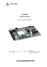
Page 1: ...IP417 Mini ITX COM Express Type 10 R3 0 Carrier Board User s Manual Version 1 0 July 2019...

Page 2: ...o the products described in this document without prior notice Every effort has been made to ensure the information in the document is correct however IBASE does not guarantee this document is error f...

Page 3: ...er s instructions may cause harmful interference to radio communications WEEE This product must not be disposed of as normal household waste in accordance with the EU directive of for waste electrical...

Page 4: ...avy objects on the top of this product Anti static precautions Wear an anti static wrist strap to avoid electrostatic discharge Place the PCB on an anti static kit or mat Hold the edges of PCB when ha...

Page 5: ...ERS SHALL BE BILLED FOR REPAIR AND SHIPPING CHARGES Technical Support Services 1 Visit the IBASE website at www ibase com tw to find the latest information about the product 2 If you need any further...

Page 6: ...g the Jumpers 8 2 2 1 How to Set Jumpers 8 2 2 Connector Locations on IP417 9 2 3 Jumpers Quick Reference 10 2 3 1 BIOS Boot Selection JP1 JP9 10 2 3 2 COM1 RS 232 Power Selection JP2 11 2 3 3 COM2 RS...

Page 7: ...ower Connector J6 15 2 4 3 COM3 COM4 Ports J13 J8 15 2 4 4 GPIO Connector J17 16 2 4 5 System Function Connector J11 16 2 4 6 DC In 12V Power Connector J14 17 2 4 7 COM1 COM2 Ports CN2 17 2 4 8 LVDS C...

Page 8: ...viii IP417 User s Manual This page is intentionally left blank...

Page 9: ...1 Chapter 1 General Information The information provided in this chapter includes Features Specifications Board Overview Board Dimensions...

Page 10: ...easures 170mm x 170mm COM Express Modules are designed for the needs of IoT embedded applications including amusement gaming ATM POS medical imaging and industrial control these mini modules combine g...

Page 11: ...rd 2x2 pin connector Display Derived from COMe module ET875 1 x DisplayPort 1 x 18 24 bit dual channel LVDS or 1 x eDP Choose either one LAN 2 x RJ45 LAN ports LAN 1 Derived from COMe module LAN 2 fro...

Page 12: ...PS 2 Keyboard port 1 x PS 2 Mouse port Battery for RTC CMOS 1 x Lithium battery button cell for RTC of COMe module Expansion Slots 1 x PCIe x1 slot 2 x Mini PCIe slot Environment Temperature Operating...

Page 13: ...Name No Name 1 PS 2 Mouse Port 7 USB 2 0 Ports 2 PS 2 Keyboard Port 8 GbE LAN Ports 3 COM1 RS 232 Port 9 Microphone Input 4 COM2 RS 232 Ports 10 Audio Line Out 5 USB 3 0 Port 11 Audio Line In 6 Displa...

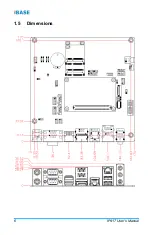
Page 14: ...6 IP417 User s Manual 1 5 Dimensions...

Page 15: ...dware Configuration This section provides information on jumper settings and connectors on the board in order to set up a workable system Jumper and connector locations Jumper settings and information...

Page 16: ...a non conductive base mounted on the circuit board Jumper caps are used to have the functions and features enabled or disabled If a jumper has 3 pins you can connect either PIN1 to PIN2 or PIN2 to PIN...

Page 17: ...Hardware Configuration IP417 User s Manual 9 2 2 2 Connector Locations on IP417 Board diagram of IP417...

Page 18: ...P4 eDP LVDS Function Setting JP5 LVDS Panel Power JP6 eDP Panel Power JP7 LVDS Backlight Power Selection JP8 eDP Backlight Power Selection JP10 AT ATX Mode Selection JP11 2 3 1 BIOS Boot Selection JP1...

Page 19: ...2 COM1 RS 232 Power Selection JP2 Function Pin closed Illustration 12V 1 3 6 5 2 1 Normal default 3 4 6 5 2 1 5V 3 5 6 5 2 1 2 3 3 COM2 RS 232 Powr Selection JP3 Function Pin closed Illustration 12V 1...

Page 20: ...5VSB default 1 2 1 5V 2 3 1 2 3 5 eDP LVDS Function Setting JP5 Function Pin closed Illustration eDP default 1 2 1 LVDS 2 3 1 2 3 6 LVDS Panel Power JP6 Function Pin closed Illustration 3 3V default...

Page 21: ...lection JP8 Function Pin closed Illustration 3 3V default 1 2 1 5V 2 3 1 2 3 9 eDP Backlight Power Selection JP10 Function Pin closed Illustration 5V default 1 2 1 12V 2 3 1 2 3 10 AT ATX Mode Selecti...

Page 22: ...em Function Connector J11 Mini PCIe Slot J12 J15 DC In 12V Power Connector J14 DisplayPort CN1 COM1 COM2 RS 232 Ports CN2 USB 3 0 CN3 PS 2 Keyboard Mouse CN4 Audio Connector CN5 GbE LAN Port CN6 CN8 U...

Page 23: ...nal Name 1 5V 3 Ground 2 Ground 4 12V 2 4 2 LVDS Panel Inverter Power Connector J6 1 Pin Signal Name Pin Signal Name 1 12V 3 ADJ 2 Backlight Enable 4 Ground 2 4 3 COM3 COM4 Ports J13 J8 1 2 9 10 Pin S...

Page 24: ...provide light indication of computer activities and switches to change the computer status It provides interfaces for the following functions ATX Power ON Switch Pins 1 and 2 The 2 pins make an ATX P...

Page 25: ...connector connects to the system power LED on control panel This LED will light when the system turns on 2 4 6 DC In 12V Power Connector J14 3 4 1 2 Pin Signal Name Pin Signal Name 1 Ground 3 12V 2 Gr...

Page 26: ...tor supports single channel 18 bit or 24 bit displays 1 2 19 20 Pin Signal Name Pin Signal Name 1 TX0P 2 TX0N 3 Ground 4 Ground 5 TX1P 6 TX1N 7 Ground 8 Ground 9 TX2P 10 TX2N 11 Ground 12 Ground 13 CL...

Page 27: ...18 EDP Power 4 Backlight Power 19 EDP Power 5 Backlight Power 20 Ground 6 N C 21 AUXN 7 N C 22 AUXP 8 Backlight CTRL 23 Ground 9 Backlight Enable 24 TX0P 10 Ground 25 TX0N 11 Ground 26 Ground 12 Grou...

Page 28: ...20 IP417 User s Manual This page is intentionally left blank...

Page 29: ...21 Appendix This section provides the mapping addresses of peripheral devices the sample code of watchdog timer configuration and types of on board connectors...

Page 30: ...DF20F 20DP 1V HRS DF20A 20DS 1C DC in 12V Power Connector J14 Hao Guo Xing Ye ATX4PT NY46 Molex 39 01 2040 Digital I O Connector J17 Hao Guo Xing Ye DF11 10S PA66H HRS DF11 10DS 2C Panel Inverter Powe...

Reviews: