background image

SERVICE MANUAL

No.82923

June 2002

VIDEO CASSETTE RECORDER

SPECIFICATIONS

 (The specifications shown pertain specifically to the model HR-S7950EU.)

This service manual is printed on 100% recycled paper.

COPYRIGHT © 2002 VICTOR COMPANY OF JAPAN, LTD

HR-S6950EU, HR-S6955MS, 

HR-S7950EU, HR-S7955EK, HR-S7955MS

V15S1/S2/S15

GENERAL

Power requirement : AC 220 V – 240 V

d

, 50 Hz/60 Hz

Power consumption

Power on

: 18 W

Power off

: 3.6 W

Temperature

Operating

: 5

°

C to 40

°

C

Storage

: –20

°

C to 60

°

C

Operating position : Horizontal only
Dimensions (WxHxD)

: 400 mm x 94 mm x 270 mm 

Weight

: 3.4 kg

Format

: S-VHS/VHS PAL standard

Maximum recording time

(SP)

: 240 min. with E-240 video cassette

(LP)

: 480 min. with E-240 video cassette

(EP)

: 720 min. with E-240 video cassette

VIDEO/AUDIO

Signal system

: PAL-type colour signal and CCIR 

monochrome signal, 625 lines 
50 fields

Recording system : DA4 (Double Azimuth) head helical 

scan system

Signal-to-noise ratio: 45 dB
Horizontal resolution

(SP/LP)

: 250 lines (VHS)

400 lines (S-VHS)

(EP)

: 220 lines (VHS)

350 lines (S-VHS)

Frequency range

: 70 Hz to 10,000 Hz (Normal audio)

20 Hz to 20,000 Hz (Hi-Fi audio)

Input/Output

: 21-pin SCART connectors:

IN/OUT x 1, IN/DECODER x 1
RCA connectors:
VIDEO IN x 1, AUDIO IN x 1,


AUDIO OUT x 1
S-Video connector:
IN x 1, OUT x 1

TUNER/TIMER

TV channel storage capacity

: 99 positions (+AUX position)

Tuning system

: Frequency synthesized tuner

Channel coverage : VHF 47 MHz – 89 MHz/

104 MHz – 300 MHz/
302 MHz – 470 MHz
UHF 470 MHz – 862 MHz

Aerial output

: UHF channels 22 – 69 (Adjustable)

Memory backup time

: Approx. 10 min.

ACCESSORIES

Provided accessories

: RF cable,

Infrared remote control unit,
“R6” battery x 2

Specifications shown are for SP mode unless otherwise 
specified.
E.& O.E. Design and specifications subject to change without 
notice.

www.freeservicemanuals.info

3/28/2017

Digitized in Heiloo Netherland

Summary of Contents for HR-S6950EU

Page 1: ...gnal 625 lines 50 fields Recording system DA4 Double Azimuth head helical scan system Signal to noise ratio 45 dB Horizontal resolution SP LP 250 lines VHS 400 lines S VHS EP 220 lines VHS 350 lines S VHS Frequency range 70 Hz to 10 000 Hz Normal audio 20 Hz to 20 000 Hz Hi Fi audio Input Output 21 pin SCART connectors IN OUT x 1 IN DECODER x 1 RCA connectors VIDEO IN x 1 AUDIO IN x 1 AUDIO OUT x ...

Page 2: ...www freeservicemanuals info 3 28 2017 Digitized in Heiloo Netherland ...

Page 3: ...3 1 Audio REC FM 3 5 3 3 4 Syscon circuit EU EK MODEL 3 6 3 3 4 1 Timer clock 3 6 3 3 5 PAL SECAM converter circuit MS MODEL 3 6 3 3 5 1 Colour difference level 3 6 3 3 5 2 SECAM burst position 3 6 4 CHARTS AND DIAGRAMS 4 1 BOARD INTERCONNECTIONS 4 3 4 2 MAIN VIDEO N AUDIO SCHEMATIC DIAGRAM 4 5 4 3 MAIN ON SCREEN SCHEMATIC DIAGRAM 4 7 4 4 MAIN SECAM SCHEMATIC DIAGRAM HR S6950MS S7955MS 4 8 4 5 MAI...

Page 4: ...cognized codes pertaining to X ray emission Consequently when servicing these products replace the cath ode ray tubes and other parts with only the specified parts Under no circumstances attempt to modify these circuits Unauthorized modification can increase the high voltage value and cause X ray emission from the cathode ray tube 12 Crimp type wire connector In such cases as when replacing the po...

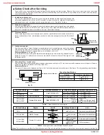
Page 5: ...als of load Z See figure 9 and following table 2 5 Grounding Class 1 model only Confirm specified or lower grounding impedance between earth pin in AC inlet and externally exposed accessible parts Video in Video out Audio in Audio out or Fixing screw etc Measuring Method Connect milli ohm meter between earth pin in AC inlet and exposed accessible parts See figure 10 and grounding specifications d ...

Page 6: ...www freeservicemanuals info 3 28 2017 Digitized in Heiloo Netherland ...
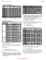
Page 7: ...any grease See Fig 1 1b In case of mechanical failures while keeping the tension arm assembly free from tension pull out the tape on the pole base assembly Take the spring a of the pinch roller arm assembly off the hook and detach it from the tape 4 Remove the screw a of the side frame L R 5 Hold the slack tape and cassette cover together lift the cassette tape top frame cassette holder and side f...

Page 8: ...ppropriately since the installation state of the Drum assembly influences the FM WAVEFORM LINEARITY greatly HOOK Note 3c When reattaching the Drum assembly secure the screws S3c to S3e in the order of c d e When handling the drum assembly alone hold it by the motor or shaft Be careful not to touch other parts especially the video heads Also take care not to damage the connectors Fig 1 2 2c Shaft V...

Page 9: ...de back side JS3001 Accord the position of V gap on R Encoder and PWB silk Phase alignment Accord the position of Boss on R Encoder and PWB silk For the prevention of the DRUM FPC damage When you attach the Mechanism assembly on Bottom chassis Attach the Mechanism assembly after the positioning boss z of the Bottom chassis is matched to the positioning hole of the Mehcanism assembly S5a S5b S5b S5...

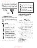
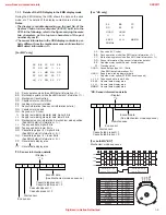
Page 10: ...splay E Latest Previous See 1 3 4 EMG code display mode Normal display Counter or clock Reference EMG display of FDP display mode 1 Transmit the code 59 from the Jig RCU The FDP shows the EMG content in the form of E Example 1 E 01 03 Previous EMG Latest EMG No EMG record Example 2 E 2 Transmit the code 59 from the Jig RCU again The FDP shows the EMG detail information 1 in the form of 1 2 34 1 De...

Page 11: ...higher 8 bits MM Tape speed data lower 8 bits NN Cassette tape type 2 higher 8 bits See EMG detail of information 2 OO Cassette tape type 2 lower 8 bits See EMG detail of information 2 P P General data display area Y Y General data display area For HD only AA BB CC DD EE FF GGGG HHHH I I J J J J KKKK L L L L MMMM ROM No Display h Encoder data See Mechanism mode sequence Remote pause End sensor Sta...

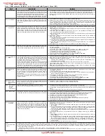
Page 12: ...eel sensor failure 3 Power SW5V is not supplied to the reel sensor on the tape winding side 1 The drum could not start or the drum rotation has stopped due to too large a load on the tape because 1 The tape tension is abnormally high 2 The tape is damaged or a foreign object grease etc adheres to the tape 2 The drum FG pulse did not reach the System controller CPU because 1 The signal circuit is d...

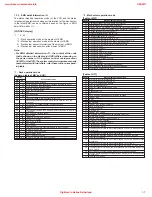
Page 13: ...REC 43 REW 47 REV SEARCH 4C AUDIO DUB 6E INSERT REC VIDEO AUDIO 84 FWD STILL SLOW 85 REV STILL SLOW 8F REC PAUSE AF INSERT REC PAUSE C7 REV SEARCH x1 speed reverse playback using JOG CD AUDIO DUB PAUSE EF INSERT REC VIDEO AUDIO PAUSE F0 Mechanism being initialized F1 POWER OFF as a result of EMG F2 Cassette being inserted F3 Cassette being ejected F4 Transition from STOP with pinch roller pressure...

Page 14: ...g the remaining tape detection function of the cas sette tape As a result it may not identify cassette correctly when a special cassette tape is used or when the tape has variable thickness 1 3 6 EMG detail information 2 The type of the cassette tape and the cassette tape winding posi tion can be confirmed based on the figure in EMG detail informa tion 2 FDP OSD display 5 6 7 5 Type of the cassett...

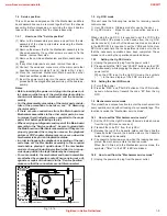
Page 15: ...t a di agnosis or repair of the boards in the Service position make sure that the connectors are not disconnected Fig 1 4 1a 1 6 Mechanism service mode This model has a unique function to enter the mechanism into every operation mode without loading of any cassette tape This function is called the Mechanism service mode 1 6 1 How to set the Mechanism service mode 1 Set the VCR to the Jig RCU mode ...

Page 16: ...acement If any oil or grease on con tact parts is soiled wipe it off and newly lubricate the parts Note See the mechanism assembly diagram of the parts list for the lubricating or greasing spots and for the types of oil or grease to be used 1 7 3 Suggested servicing schedule for main components The following table indicates the suggested period for such service measures as cleaning lubrication and...

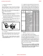
Page 17: ...are hooked all the way around and in the correct direction When performing repairs take care not to damage a catch etc Fig 2 1 1a Fig 2 1 3a 2 1 2 Mechanism operation check When the mechanism is operated without a cassette loaded operate the mechanism in the mechanism service mode Re fer to the section 1 disassembly 2 1 3 Setting the mechanism assembling mode The mechanism assembling mode is provi...

Page 18: ... T12 Idler arm T13 Reel disk supply side T14 Rec safety lever T15 Tension arm base T16 Tension arm assy T17 Full erase head T11 Ider gear 1 2 B1 Load gear assy take up side B2 Fixing plate B3 Load gear assy supply side B4 Load gear B5 Control plate B6 Tension arm lever B7 Change lever B8 Clutch unit assy B9 Loading motor assy B10 Belt B11 Control cam B12 Press lever B13 Capstan brake B14 Capstan m...

Page 19: ...2 3 4 2 1 Side frame R T 3 1 2 2 2 A C head T 1 FE head T B 1 2 3 Guide arm assy T 1 2 3 Lid guide T 1 2 3 Pinch roller arm assy T 2 1 2 4 Idler arm T 4 1 2 3 2 4 Idler gear 1 2 T 5 1 2 3 4 2 5 Main brake assy T T 6 1 2 3 4 5 2 5 Reel disk T T 7 1 2 3 4 5 6 2 5 T ension arm T 6 1 2 3 4 5 2 5 Reel disk S T 7 1 2 3 4 5 2 5 T ension arm base T 7 1 2 3 4 5 T up head T 8 1 2 3 4 5 T up lever T 8 1 2 3 ...

Page 20: ...f the loading motor assembly so that the main deck connects to the guide hole a of the drive lever 2 Place the projection of the drive lever on section a of the side frame R and install the side frame R to the main deck 3 Secure screw b 4 Place section b of the drive arm on the gear of the side frame R Make sure that the pin of the door opener con nects with section c of the drive arm 5 Place the ...

Page 21: ...order of c d and e To make the adjustment easy tem porarily elevate the A C head Fig 2 2 2a Fig 2 2 2b Guide hole a Cassette Holder Assembly Gear a Screw a Section b Section c DRIVE ARM L SIDE FRAME L Section d DRIVE ARM R SIDE FRAME R Section a Screw b DRIVE LEVER SIDE FRAME R EARTH SPRING 1 Hook a TOP FRAME Position guide a Arrow a HEAD BASE Screw a Screw c Screw d Screw e Screw b Spring a A C H...

Page 22: ...and turn section b of the brake lever counterclockwise to remove the brake lever 5 Remove the spring b from the hook a 6 Release the catch c to detach the tension arm 7 Release the catch d to detach the reel disk S and the spacer 8 Remove the spring c from the hook b 9 Turn the tension arm base in the direction shown by arrow a to release catch e Place the projections of the tension arm base to th...

Page 23: ...bly BRAKE LEVER Main brake T assembly Catch a Catch b Section b Spring b Hook a Catch d Catch c Tension arm assembly REEL DISK S REEL DISK T REEL DISK T REEL DISK S Tension arm assembly Tension arm base assembly BRAKE LEVER REC SAFETY LEVER SPACER Spring c Catch f Tension arm base assembly Catch e Hole a Hole a Arrow a Hook b REC SAFETY LEVER Catch d Catch c Screw a Screw a Loading motor assembly ...

Page 24: ...tall the control cam 9 Move the capstan brake in the direction shown by the arrow a to attach the press lever to the shaft a Make sure that the boss of the press lever fits in the control cam and that the shaft b of the pinch roller arm assembly connects with the hole of the press lever 10 Attach slit washer a to shaft a Fig 2 2 6b Fig 2 2 7a Screw a Shaft a Shaft b PRESS LEVER Slit washer a Arrow...

Page 25: ... hole g of the control plate 8 Attach the load gear on the load gear base so that the con trol plate is placed on the edge h of the load gear 9 Place the fixing plate on the shaft of the load gear base and secure the screws b Fig 2 2 7b 2 2 8 Clutch unit assembly direct gear 2 2 8 1 Removal 1 Remove the slit washer a to detach the clutch unit assem bly 2 Remove the spring a and the direct gear Fig...

Page 26: ...PLAY STOP MODE PRESS UP STOP REV OFF OFF OFF OFF ON OFF FF REW EJECT PLAY FOR SLOW STILL REV SERCH SLOW STILL FF REW STOP REEL BRAKE ON ON OFF ON ON OFF OFF2 OFF1 ON CLUTCH DIRECT Movements of a CONTROL PLATE m m 0 5 15 20 25 30 35 40 45 50 55 10 CONTROL PLATE MARK E P SL R ST B FR MECHANISM MODE CONTACT www freeservicemanuals info 3 28 2017 Digitized in Heiloo Netherland ...

Page 27: ...ed test equipments Color colour television or monitor Oscilloscope wide band dual trace triggered delayed sweep Signal generator RF IF sweep marker Signal generator stairstep color colour bar PAL SECAM Recording tape Digit key remote controller provided 75 White 75 0 7 V 0 3 V Horizontal sync V U 1V White 100 Yellow Cyan Green Magenta Red Blue Burst 0 3 V V R Y U B Y White Yellow Cyan Green Magent...

Page 28: ...stment prepare a cassette tape for self recording play back perform a test on it by transporting it and making sure that the tape is not bent by the tape transport mechanisms such as in the guide rollers See Fig 3 2 2a 3 2 1 Tension pole position Signal A Back tension cassette gauge PUJ48076 2 Mode B1 Play back position B2 Eject end Adjustment part F Adjust pin Mechansim assembly Specified value G...

Page 29: ...lat V PB FM waveform Adjustment tool H Roller driver PTU94002 1 Play back the alignment tape A1 2 Apply the external trigger signal to D FF E to observe the V PB FM waveform at the measuring point D 3 Set the VCR to the manual tracking mode 4 Make sure that there is no significant level drop of the V PB FM waveform caused by the tracking operation with its generally parallel and linear variation e...

Page 30: ... A C head See Fig 3 2 4a 5 Rotate the roller driver so that the A C head comes clos est to the capstan From there move the A C head back gradually toward the drum until the point where the FM waveform is maximized for the second time and then tighten the screws 4 and 5 temporarily 6 Play an alignment tape A2 and set to the manual track ing mode 7 Fine adjust A C head base position to maximize the ...

Page 31: ...p p 1 Apply the external trigger signal to D FF E to observe the Audio PB FM waveform at the measuring point D 2 Record the signal A3 with no audio signal input in the mode B and play back the recorded signal 3 Set the VCR to the manual tracking mode 4 If the A PB FM level is not within the specified value G1 perform the adjustment in a following procedure 5 Adjust the Adjustment part F so that th...

Page 32: ...djustment part F1 VR1602 B Y ADJ F2 VR1601 R Y ADJ Specified value G1 460 20 mVp p B Y G2 620 20 mVp p R Y 3 3 5 PAL SECAM converter circuit MS MODEL Note Unless otherwise specified in this P S Converter cir cuit adjustments all measuring points and adjustment parts are located on the S P Converter board Fig 3 5 1a Colour difference level GREEN YELLOW BLUE MAGENTA H rate Specified value G2 Specifi...

Page 33: ...www freeservicemanuals info 3 28 2017 Digitized in Heiloo Netherland ...
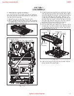
Page 34: ...VICTOR COMPANY OF JAPAN LIMITED VIDEO DIVISION Printed in Japan S40894 www freeservicemanuals info 3 28 2017 Digitized in Heiloo Netherland ...
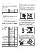
Page 35: ...ION LPT0650 015A INST BOOK HU A LPT0650 016A INST BOOK RU A LPT0651 001A INST BOOK EN C LPT0651 002A INST BOOK GE C LPT0651 003A INST BOOK FR C LPT0651 004A INST BOOK DU C LPT0651 005A INST BOOK SP C LPT0651 006A INST BOOK IT C LPT0651 007A INST BOOK DA C LPT0651 008A INST BOOK FI C LPT0651 009A INST BOOK SW C LPT0651 010A INST BOOK NO C LPT0651 011A INST BOOK PT C LPT0651 012A INST BOOK GR C LPT0...

Page 36: ...ch the Mechanism assembly on Bottom chassis Attach the Mechanism assembly after the positioning boss z of the Bottom chassis is matched to the positioning hole of the Mehcanism assembly 532 MAIN BOARD ASSY 03 533 533 533 517 Insert the bushing of POWER CORD so as not to twist the cord a d d g e 520 522 521 MECHANISM ASSY M4 505 510 510 510 515 516 516 525 519A 519 g NOTE AFTER ATTACHED ROLLER ARM ...

Page 37: ...QYTDSF4012Z SCREW MECHA 516 QYSPSFG3010Z SCREW X2 MECHA 517 QMP4A10 170 POWER CORD A B C E QMP51K0 170 K POWER CORD D 519 LP40370 001F ROLLER ARM ASSY 519A PDM4311A 1 ROLLER ASSY 520 PQ45160 INERTIA PLATE 521 PQM30017 51 SLIT WASHER 522 QYSLSF2060D SCREW 525 LP40700 001A SPECIAL SCREW MECHA 529 LP31019 005C KNOBASSY B C D E LP31019 005D KNOB ASSY A 530 QYTPSFG2608Z SCREW X2 ADJ JOG 531 QYTDSF2608Z...

Page 38: ...7 112 123 151 113 115 124 125 79 82 21 4 117 44 26 3 58 52 57 58 55 90 37 77 72 116 50 112 122 110 126 126 89 36 73 69 102 70 134 78 76 71 120 42 85 46 47 81 83 80 49 119 53 111 114 118 121 96 93 94 95 64 51 65 18A 19 22 20 16 23A 63 66 59 62 68 24 18 84 61 60 67 23 23B 18B WR2 A C HEAD BOARD ASSY 12 LOADING MOTOR BOARD ASSY 55 48 AA AA AA AA AA AA AA AA AA AA AA AA AA BB BB BB BB BB AA AA AA AA A...

Page 39: ...N ARM ASSY 72 LP40844 001D TENSION SPRING 73 LP21045 001D TENSION ARM BASE 74 LP40821 001A TENSION BAND ASSY 75 LP30967 001B BAND HOLDER 1 76 LP30968 001C BAND HOLDER 2 77 LP40822 002B ADJUST PIN 78 LP31000 005E TENSION ARM LEVER 79 LP21046 001C MAIN BRAKE TAKE UP 80 LP40824 001A BAND BRAKE ASSY 81 LP30969 002A BRAKE LEVER 82 LP30003 033B TENSION SPRING 83 LP30003 035B TENSION SPRING 84 LP40825 00...

Page 40: ...144WU DIGI TRANSISTOR B E or RN1309 DIGI TRANSISTOR B E or UN521E DIGI TRANSISTOR B E Q21 2SA1576A QR X TRANSISTOR or 2PA1576 R X TRANSISTOR Q24 2SA1576A QR X TRANSISTOR or 2PA1576 R X TRANSISTOR Q25 DTC144WU DIGI TRANSISTOR C D or PDTC144WU DIGI TRANSISTOR C D or RN1309 DIGI TRANSISTOR C D or UN521E DIGI TRANSISTOR C D Q38 2SC4081 QRS X TRANSISTOR or 2PC4081 R X TRANSISTOR Q40 DTC144WU DIGI TRANS...

Page 41: ...211 DIGI TRANSISTOR Q3002 PTZ NV16A PHOTO TRANSISTO Q3003 PTZ NV16A PHOTO TRANSISTOR Q3004 2SD1819A QRS X TRANSISTOR or 2PC4081 R X TRANSISTOR or 2SC4081 QRS X TRANSISTOR Q3005 2SD1819A QRS X TRANSISTOR or 2PC4081 R X TRANSISTOR or 2SC4081 QRS X TRANSISTOR Q3007 UN521E DIGI TRANSISTOR or DTC144WU DIGI TRANSISTOR or PDTC144WU DIGI TRANSISTOR or RN1309 DIGI TRANSISTOR Q4001 UN5211 DIGI TRANSISTOR or...

Page 42: ...C ZENER DIODE or RD5 6ES B3 T2 ZENER DIODE D6002 HZ30 2L T2 ZENER DIODE or HZ30 2LTD Z DIODE M D7051 1SS133 DIODE or 1SS270A DIODE R1 NRSA02J 622X MG RESISTOR 6 2kØ 1 10W R2 NRSA02J 152X MG RESISTOR 1 5kØ 1 10W R3 NRSA02J 182X MG RESISTOR 1 8kØ 1 10W R5 NRSA02J 0R0X MG RESISTOR 0Ø 1 10W R6 NRSA02J 273X MG RESISTOR 27kØ 1 10W R7 NRSA02J 681X MG RESISTOR 680Ø 1 10W R10 QRE141J 103Y RESISTOR 10kØ 1 4...

Page 43: ...NRSA02J 473X MG RESISTOR 47kØ 1 10W R2060 NRSA02J 183X MG RESISTOR 18kØ 1 10W R2061 NRSA02J 273X MG RESISTOR E 27kØ 1 10W R2062 NRSA02J 3R3X MG RESISTOR E 3 3Ø 1 10W R2063 QRE141J 151Y RESISTOR E 150Ø 1 4W R2064 NRSA02J 473X MG RESISTOR E 47kØ 1 10W R2065 NRSA02J 183X MG RESISTOR E 18kØ 1 10W R2201 NRSA02J 473X MG RESISTOR 47kØ 1 10W R2202 NRSA02J 682X MG RESISTOR 6 8kØ 1 10W R2203 NRSA02J 473X MG...

Page 44: ...1 10W R3096 NRSA02J 0R0X MG RESISTOR 0Ø 1 10W R3097 NRSA02J 0R0X MG RESISTOR 0Ø 1 10W R3103 NRSA02J 0R0X MG RESISTOR 0Ø 1 10W R3104 NRSA02J 0R0X MG RESISTOR E 0Ø 1 10W R3105 NRSA02J 0R0X MG RESISTOR 0Ø 1 10W R3106 NRSA02J 0R0X MG RESISTOR 0Ø 1 10W R3205 QRE141J 181Y RESISTOR 180Ø 1 4W R3206 NRSA02J 123X MG RESISTOR 12kØ 1 10W R3207 NRSA02J 183X MG RESISTOR 18kØ 1 10W R3208 NRSA02J 121X MG RESISTOR...

Page 45: ...04 QUY160 080Y IM BUS WIRE B214 NRSA02J 0R0X MG RESISTOR 0Ø 1 10W B302 NRSA02J 0R0X MG RESISTOR B E 0Ø 1 10W B2051 QUY153 050Y IM BUS WIRE B QUY160 060Y IM BUS WIRE A C D B2221 QUY160 140Y IM BUS WIRE B5001 QUY160 100Y IM BUS WIRE B5002 QUY160 100Y IM BUS WIRE B7001 NRSA02J 0R0X MG RESISTOR 0Ø 1 10W C1 NCB21EK 104X CAPACITOR E 0 1µF 25V NCB21HK 103X CAPACITOR A B C D 0 01µF 50V C2 NCB21EK 104X CAP...

Page 46: ...75 E CAPACITOR 4 7µF 50V C2013 NCB21HK 331X CAPACITOR 330pF 50V C2017 NCB21HK 682X CAPACITOR 0 0068µF 50V C2051 NCB21HK 331X CAPACITOR 330pF 50V C2052 QFLC1HJ 333Z F CAPACITOR E 0 033µF 50V C2053 NCB21HK 332X CAPACITOR E 0 0033µF 50V NCB21HK 472X CAPACITOR A B C D 0 0047µF 50V C2054 NCB21EK 223X CAPACITOR A B C D 0 022µF 25V NCB21HK 103X CAPACITOR E 0 01µF 50V C2055 QEKJ1EM 106 E CAPACITOR 10µF 25...

Page 47: ... 106 E CAPACITOR A C D 10µF 25V C6502 NCB21HK 103X CAPACITOR 0 01µF 50V C7011 QEKJ0JM 476 E CAPACITOR 47µF 6 3V C7165 NCB21HK 681X CAPACITOR 680pF 50V C7167 NCB21HK 681X CAPACITOR 680pF 50V C7202 QETJ0JM 477 E CAPACITOR 470µF 6 3V L1 QQL29BJ 100Z COIL 10µH L2 QQL071J 121Y COIL 120µH L3 QQL29BJ 100Z COIL 10µH L4 QQL29BJ 100Z COIL 10µH L5 QQR0521 012Z NOISE FILTER L12 QQR0967 001 COIL 12µH L13 QQL07...

Page 48: ...TOR 39kØ 1 10W R1211 NRVA02D 153X CMF RESISTOR 15kØ 1 10W R1212 NRSA02J 102X MG RESISTOR 1kØ 1 10W R1213 NRSA02J 331X MG RESISTOR 330Ø 1 10W R1214 NRSA02J 121X MG RESISTOR 120Ø 1 10W R1215 NRSA02J 102X MG RESISTOR 1kØ 1 10W R1216 NRSA02J 331X MG RESISTOR 330Ø 1 10W R1217 NRVA02D 101X CMF RESISTOR 100Ø 1 10W R1218 NRVA02D 301X CMF RESISTOR 300Ø 1 10W R1220 NRSA02J 561X MG RESISTOR 560Ø 1 10W R1222 ...

Page 49: ...10W VR1401 QUY153 050Y IM BUS WIRE B1401 NRSA02J 0R0X MG RESISTOR 0Ø 1 10W B1412 NRSA02J 0R0X MG RESISTOR 0Ø 1 10W C1401 QEKJ1CM 336 E CAPACITOR 33µF 16V C1403 QEKJ0JM 337 E CAPACITOR 330µF 6 3V C1404 NCF21EZ 104X CAPACITOR 0 1µF 25V C1405 NCF21EZ 104X CAPACITOR 0 1µF 25V C1406 NCB21HK 103X CAPACITOR 0 01µF 50V C1407 NDC21HJ 680X CAPACITOR 68pF 50V C1408 NDC21HJ 330X CAPACITOR 33pF 50V C1410 QEKJ1...

Page 50: ...R510 NRVA02D 102X CMF RESISTOR 1kØ 1 10W R511 NRVA02D 471X CMF RESISTOR 470Ø 1 10W R512 NRVA02D 102X CMF RESISTOR 1kØ 1 10W R513 NRVA02D 152X CMF RESISTOR 1 5kØ 1 10W R514 NRVA02D 332X CMF RESISTOR 3 3kØ 1 10W R515 NRVA02D 332X CMF RESISTOR 3 3kØ 1 10W R516 QUY160 100Y IM BUS WIRE R517 QUY160 100Y IM BUS WIRE R525 QRE141J 125Y RESISTOR 1 2MØ 1 4W R527 NRSA02J 332X MG RESISTOR A C D 3 3kØ 1 10W R53...

Page 51: ...E 0 01µF 50V C566 NCB21HK 103X CAPACITOR B E 0 01µF 50V C568 NDC21HJ 680X CAPACITOR 68pF 50V C569 NDC21HJ 680X CAPACITOR 68pF 50V C570 NDC21HJ 680X CAPACITOR 68pF 50V C571 NDC21HJ 680X CAPACITOR 68pF 50V C572 NDC21HJ 680X CAPACITOR 68pF 50V C573 NDC21HJ 680X CAPACITOR 68pF 50V C575 NDC21HJ 101X CAPACITOR 100pF 50V C901 NCB21HK 331X CAPACITOR 330pF 50V C902 NCB21HK 331X CAPACITOR 330pF 50V C903 NCB...

Page 52: ... 10kØ 1 4W R6720 NRSA02J 562X MG RESISTOR 5 6kØ 1 10W R6721 NRSA02J 562X MG RESISTOR 5 6kØ 1 10W C6701 NCB21HK 103X CAPACITOR 0 01µF 50V C6704 NCB21HK 103X CAPACITOR 0 01µF 50V C6707 NDC21HJ 470X CAPACITOR 47pF 50V C6708 NDC21HJ 7R0X CAPACITOR 7pF 50V C6709 NDC21HJ 3R0X CAPACITOR 3pF 50V C6713 NCF21CZ 224X CAPACITOR 0 22µF 16V C6714 NCB21HK 222X CAPACITOR A C D 0 0022µF 50V NCB21HK 682X CAPACITOR ...

Page 53: ...Ø 1 10W R1618 NRSA02J 103X MG RESISTOR 10kØ 1 10W R1619 NRSA02J 134X MG RESISTOR 130kØ 1 10W R1620 NRSA02J 332X MG RESISTOR 3 3kØ 1 10W R1621 QRE141J 103Y RESISTOR 10kØ 1 4W R1622 QRE141J 103Y RESISTOR 10kØ 1 4W R1623 NRSA02J 123X MG RESISTOR 12kØ 1 10W R1624 NRSA02J 124X MG RESISTOR 120kØ 1 10W R1631 NRSA02J 561X MG RESISTOR 560Ø 1 10W R1632 NRSA02J 332X MG RESISTOR 3 3kØ 1 10W R1633 NRSA02J 223X...

Page 54: ...CAPACITOR 0 01µF 50V C1644 NCB21HK 103X CAPACITOR 0 01µF 50V C1645 QEKJ1HM 105 E CAPACITOR 1µF 50V C1646 QEKJ1HM 105 E CAPACITOR 1µF 50V C1647 NCB21CK 224X CAPACITOR 0 22µF 16V C1648 QEKJ0JM 476 E CAPACITOR 47µF 6 3V C1649 NCB21HK 103X CAPACITOR 0 01µF 50V C1650 NCB21CK 224X CAPACITOR 0 22µF 16V C1651 NCB21EK 223X CAPACITOR 0 022µF 25V C1652 NDC21HJ 120X CAPACITOR 12pF 50V C1653 NCB21CK 224X CAPAC...

Page 55: ...IR monochrome signal 625 lines 50 fields Recording system DA4 Double Azimuth head helical scan system Signal to noise ratio 45 dB Horizontal resolution SP LP 250 lines VHS 400 lines S VHS EP 220 lines VHS 350 lines S VHS Frequency range 70 Hz to 10 000 Hz Normal audio 20 Hz to 20 000 Hz Hi Fi audio Input Output 21 pin SCART connectors IN OUT x 1 IN DECODER x 1 RCA connectors VIDEO IN x 1 AUDIO IN ...

Page 56: ...mal VHS mode 2 Audio circuits REC 1KHz 8 dBs sine wave signal in SP mode normal VHS mode PB REC then playback it 3 Movie Camera circuits Measured using a correctly illuminated gray scale or colour bar test chatrs in the E E mode 4 Indication on schematic diagram Waveform indications on the schematic diagram are as shown below 5 Waveform indications Waveform number WF25 REC PB 1 2 Vp p 50 mV 2 msec...

Page 57: ...te the signal path as follows Playback signal path Playback and recording signal path Recording signal path including E E signal path Capstan servo path Drum servo path Example R Y Y Playback R Y signal path Recording Y signal path 7 Indication of the parts for adjustments The parts for the adjustments are surrounded with the circle as shown below 8 Indication of the parts not mounted on the circu...

Page 58: ...2002 COMMON COMMON SP CH1 CN7005 JSA I2C I2C DATA CLK TU A MUTE DEMOD DEMOD R L SW5V GND COMP SIF NC GND C FROM DIGI KILLER DET I2C CLK A V I2C DATA A V CNR H VPCTL V REF D FF FH625 L TRICK H 3 58NTSC L SLOW PULSE 0 5 2D DIGITAL Page 4 21 CN1201 MINI FRONT 2 CN501 8 GND JSB JSA FRONT FRONT J7105 GND JSB JSB CN7003 CN7004 CN7002 for 400EA 400H 400HA 400HA2 3 8 2 8 O O O X X X ADV_JOG MINI_FRONT FRO...

Page 59: ... QR 2SB1218A QR 2PA1576 R DTC144WUA PDTC144WUA UN521E RN1309 6 3 QQR0657 019 PDTC144WUA UN521E RN1309 DTC144WUA OPEN NQR0360 003X OPEN OPEN OPEN OPEN OPEN OPEN OPEN 6 3 OPEN DTC144WUA PDTC144WU UN521E RN1309 NQL103K R10X NQL103K R10X OPEN NQR0403 003X 2SC4081 QRS 2SD1819A QRS 2PC4081 R 2SC4081 QRS 2SD1819A QRS 2PC4081 R 25 OPEN 2SA1576A QR 2SB1218A QR 2PA1576 R EE L 2SC4081 QRS 2SD1819A QRS 2PC408...

Page 60: ...he Schematic Diagram are for references only When replacing the parts refer to the Parts List Note SHORT TO p30088001a_rev0 C322 C315 R318 L304 SECAM_PB_COLOR SECAM_DET SECAM_REC_COLOR V_TO_OSD SW5V C SYNC GND Fsc SECAM H R328 R329 C313 R326 R327 C302 C306 C319 EE L PB_FM C324 Q303 R317 B302 L301 C323 Q301 R314 R302 C303 C304 C309 C305 C310 C311 L302 R303 C307 R305 R308 R307 R306 B301 Q311 Q312 R3...

Page 61: ... 6 8k 6 8k 6 8k 100 4 7k 4 7k 1 2k 3 3k 4 7k 1k 10 10 680 680 100p 2 7k 2 7k 0 01 2 2K 10k 4 7k 2 7k 2 7k 0 33 100p 510 0 047 4 7k 510 0 047 27k 39k 39k 27k AN3651FBP 25 25 6 3 50 50 25 25 25 25 25 16 1SS133 50 50 16 16 16 6 3 16 OPEN SHORT DTC114EUA OPEN 6 3 6 3 A REC_FM OPEN OPEN A PB FM 2SC4081 QRS 2SC4081 QRS DTA144WUA DTC144WUA 25 25 DTC144WUA DTC144WUA DTC144WUA DTC114EUA QVP0039 103Z OPEN O...

Page 62: ... 12k 18k 12p 180 330k 470k 120 120 10k 18k 18k 18p 0 047 1 10k 10K 4 7k 10 0 1 4 7k 47 47 0 0 0 001 3300 10k 0 0 47 10k 1k 0 1k 10k 1k 1k 3 3k 3 3k 1k 100p 0 1 0 056 5 6K 4 7k 680p 10k 0 0022 0 022 0 33 10k 10k 4 7k 4 7k 100k 0 1 1k 0 0 0 0 0 01 10k 10k 0 4 7K 10K 0 001 CTL SVss CTL CTLBIAS CTLFB CTLAMPOUT CTLSMTIN CFG SVcc AVcc AVss Vss Vcc I2C_DATA I2C_CLK FWE NMI X2 X1 RES OSC1 OSC2 Vss VCC VCL...

Page 63: ... 04 10ELS4 AK04 11EQS04 1S4 SBO40 DTA114EUA UN5111 RN2302 PDTA114EU MTZJ5 6C RD5 6ES B3 AU01Z 10ELS2 QQR0678 001 QQR0621 001 SHORT 1SS133 1SS270A MY 16 2SD1858 QR 2SC1740S RS T 2SC3199 YG T PS2561L1 1 L PC123F2 ON3171 R 2W QQR0978 001 QQR0608 001 QQR0609 001 QQR0610 001 400 DTC114EUA UN5211 RN1302 PDTC114EU 1 2W 50 MY 1W 2W 2SD2144S UV QQS0083 001 QQS0084 001 QQS0093 001 50 MY 2SC5739 QP 50 RK14 2...

Page 64: ...T OUT ALPS MATSUSHITA TU_A_MUTE NC KOREA NC GND AUDIO IN CH SW MOD B SW5V CONV_CTL VIDEO IN NC GND RF AGC BT AS SCL SDA NC MB SW5V NC TU 30V IF OUT IF IN NC NC AUDIO OUT SIF OUT AFT TO DEMOD CN6701 0 3 MAIN TUNER VIDEO OUT NC OPEN PAL DEMOD_ R I2C_CLK TO FMA GND SIF COMP SW5V DEMOD_ L MS I2C_DATA p10436001a_rev0 OPEN TO VIDEO N AUDIO TO FMA TO VIDEO N AUDIO TO VIDEO N AUDIO TO ON SCREEN TO VIDEO N...

Page 65: ...14TYPE V15NEW DI7001 7 8 9 NC NC Da Da D7 D6 R7001 R7008 Q7006 Q7007 Q7015 D7001 D7002 R7009 R7010 Q7007 LED USED USED NOT USED NOT USED ONLY USED BY V14TYPE 7segLED IC7042 C7041 C7042 D7043 R7046 USED BY 360H K CN7001 TOOL 400HA2 OTHERS 1 6 3 6 GP1U291Q TO MAIN FRONT CN7001 TO MINI FRONT CN7005 MY p20280001a_rev0 CN7002 CN7005 S7028 S7029 JSB GND JSA b7 b6 JSA GND JSB b5 KEY OUT b5 KEY OUT TO ADV...

Page 66: ...SUB Y_TO_AV REC_COLOR REAR_V_IN Fsc P MUTE L C7202 R7204 R7202 R7203 L7201 Q7201 J7105 I2C_DATA_A V I2C_CLK_A V 680p 680p 100 75 100 100 470 10 220 4 7k 10µ SCR H SW12V GND I2C_CLK2 I2C_DATA2 P50_I O 3 58NTSC H P ON_P TU_VIDEO OPEN OPEN Fsc Y_FROM_DIGI GND GND Y V_TO_DIGI C_TO_DIGI C_FROM_DIGI GND GND DEC OUT R DEC OUT L GND A IN1 L A IN1 R A OUT L A OUT R A IN2 L A IN2 R SAT_CTL_OUT R PAUSE PB_CO...

Page 67: ... 100p 47 100µ 120 100 47 0 1 0 1 0 1 0 1 0 1 0 1 560 15µ 18p 56p 470 560 0 01 4 7 47 0 01 15p OPEN VREF CMUTE RESET VDD VSS IIC_CLK IIC_DATA COMP IREF IOB COUT AVSS AVDD YOUT AVSS AVDD CLP YVIN AVSS AVDD VRL VRH CIN VSS VDD FSC_IN PO VCNT AVSS AVDD NC TEST NC TEST NC TEST NC TEST NC TEST NC TEST NC TEST NC TEST NC TEST NC TEST NC TEST NC TEST SIMLD JCP8036 0 5 2SC4081 S 6 3 6 3 0 5 0 5 SHORT OPEN ...

Page 68: ...k 470 1k 1k 1k 0 1 6 8µ 68p 33p 0 1 0 1 100 100 120 33 0 01 10µ 47 1k 0 1 0 1 0 1 0 1 10µ 330 47k 47k 4 7 100p 0 5 25 2SC4081 S CH OPEN SHORT 6 3 CH CH 0 5 OPEN OPEN OPEN OPEN QQR0521 006Z 6 3 OPEN CH OPEN CH CH OPEN 50 OPEN OPEN OPEN DTC124TUA OPEN 0 5 0 5 0 5 SHORT CH CH CH OPEN 6 3 OPEN CH OPEN CH OPEN CH CH CH OPEN Fsc GND C_TO_DIGI SW5V 2 V Y_TO_DIGI EE L Y_FROM_DIGI GND C_FROM_DIGI KILLER_DE...

Page 69: ...OR GND GND V_FROM_AV Y_TO_AV SW5V SW5V SW5V FROM_PS_Y GND GND GND TO_PS_Y FROM_PS_C TO_PS_C SW12V SW12V 50 50 2 CH VC2076DP PB_COLOR FRONT_Y_IN ADJ SECAM_PB_COLOR MAIN_ALC_DET Y_TO_SUB P MUTE L FRONT_V_IN V_TO_OSD CHARA_DATA V_FROM_OSD GND GND 16 6 3 50 50 50 50 0 5 0 5 0 5 0 5 0 5 SHORT 0 5 50 50 2 CH 2 CH CH CH 2 CH 2 CH 2 CH 6 3 2 CH OPEN OPEN 6 3 0 6 TERMINAL S SUB TO S P CONVERTER TO I O TO M...

Page 70: ...0 75 75 100 470 510 100 75 0 100 75 0 0 01 100 75 15µ 0 10µH 10µH 10µH 100 100 100 100 4 7µ 4 7µ 4 7µ 0Ω 0 022 15µ 75 75 4 7µ 47 5 6k 3 3k 330p 330p 470p 5 6k 1µ 470p 330p 330p 33p 470p 470p 4 7µ 4 7µ 4 7µ 4 7µ 75 10 100 470p 47 47 1K 0Ω 0Ω 75 220 100 0 001 10 0 022 0 022 0 022 75 75 330p 330p 1µ 470p 330p 330p 100 0 22µ 470p 1k 75 100 100 10k 0 01 4 7k 0 1k 560 6 8k 2 7k 3 3k 470p 0 001 330 68 75...

Page 71: ... C6728 C6740 CN6701 R6723 L6702 R6721 R6722 C6732 Q6701 R6724 C6734 R6725 R6726 L6703 C6713 C6733 C6708 C6709 C6717 B6701 R6712 C6715 C6714 R6718 C6725 C6726 B6702 R6714 C6721 0 47 10 10 1k 1k 6800p 2 2 6800p 2 2 600 0 47 3 3 10 600 0 47 3 3 600 8 2k 0 47 10 1k 27p 10k 3 3µ 39k 0 033 0 33 39k 100 100 100p 100p 600 0 47 10 600 1 0 22 0 01 0 47 0 01 600 600 47 2 2 0 01 220p 47 1µ 3 9k 4 7K 0 01 220 ...

Page 72: ...00k 560 3 3k 1 2k 0 22 1000p 2200p 10k 470k 1 100p 130k 470k 330 1 0 01 100k 1k 10µ 1 5k 1 5k 0 01 22k 560 3 3k 47 47 0 01 10k 33k 27k 470 470 680 1k 560 2 2k 0 01 10µ 47 3 3k 0 01 0 01 470 10k 10k 1 2k 0 01 1p 100 680 330 470 1 2k 1k 1k 1k 2 7k 10µ 0 01 47k 56k 680 1 2k 680 2 2k 330 22 47 100 680 330 470 1 2k 1k B Y n c n c CVBS fref TEST GND n c SSC n c CLOCHEref PLLref n c Vp n c R Y TDA8395 SW...

Page 73: ...T2051 T2052 TP106 TP111 TP2253 TP2254 TP4001 X1 X2 X3001 X3002 R317 CP3002 W15 D5209 R2041 W41 C2018 W57 W40 W37 W38 W34 W56 W65 W43 W55 W52 W68 W48 W49 W45 R2239 R2240 W46 W36 W6 W8 W32 W42 W33 W23 W35 W30 W31 W29 W25 W61 W63 W64 W10 W19 W21 R30 R52 C41 R8 C42 R2056 K2006 ZZ1 ZZ2 ZZ3 ZZ4 ZZ5 ZZ6 ZZ7 ZZ8 ZZ9 D7051 R9 2 10 10 1 NEUTRAL BLU B E B E 1 2 E B 17 1 REC AGC E B 1 1 11 Q7001 K2001 K2002 K...

Page 74: ...C 16C Q3901 B C 15E Q4001 B C 12C Q4002 B C 9E Q4003 B C 9D Q5101 A D 2L Q5102 A D 3M Q5301 A D 4G Q5303 A D 1F Q5304 A D 3G Q5305 B C 4G Q5306 B C 4G Q5307 A D 3E Q5321 A D 1F Q6030 B C 21K Q6031 B C 21L Q6032 B C 21L Q7001 B C 10A Q7002 B C 10A Q7003 B C 11A Q7004 B C 11A Q7005 B C 11A Q7006 B C 11A Q7007 B C 12A Q7008 B C 12A Q7009 B C 12A Q7010 B C 12A Q7011 B C 13A Q7012 B C 14B Q7013 B C 14A...

Page 75: ... C1429 C1448 C1416 C1401 C1432 B1412 R1445 R1444 R1406 C1402 C1405 C1406 C1409 C1411 C1412 C1413 C1414 C1415 C1417 C1425 C1430 C1433 C1434 C1435 C1436 C1440 C1441 C1444 C1445 C1452 C1455 C1459 C1460 C1461 C1462 C1463 C1464 C1465 C1467 C1471 C1472 D1402 L1404 L1407 LC1401 LC1402 Q1401 Q1402 Q1404 R1459 Q1410 R1401 R1402 R1405 R1456 Q1415 R1408 R1410 R1411 R1412 B1401 R1415 R1416 R1417 R1418 R1425 R...

Page 76: ... 2D R928 A D 2D R929 B C 11E R930 B C 10E R931 B C 10A R932 B C 9A R933 B C 9A R934 A D 11B R935 A D 9B R936 A D 8A R937 A D 9B R938 A D 11B R939 A D 11B R940 B C 10B R941 B C 9E R942 B C 9D R943 B C 9E R944 B C 10E R945 B C 9D R946 B C 10E R947 B C 10E R949 A D 8E R951 B C 8E R952 B C 9D R953 B C 8D R961 B C 2A R962 B C 1C R963 B C 1B R964 B C 4C R965 B C 4B R966 A D 7A OTHER BT901 A D 6B COMPONE...

Page 77: ...V 1 msec DIV WF2 IC1 30 PAL PB 0 68 Vp p 20 mV 20 µsec DIV WF3 IC1 1 PB 0 3 Vp p 20 mV 5 msec DIV WF4 TP106 PB FM PB 0 5 Vp p 20 mV 5 msec DIV WF5 TP111 D FF REC PB 3 4 Vp p 0 1 V 10 msec DIV WF1 IC1 27 PB 2 1 Vp p 50 mV 20 µsec DIV VIDEO WF7 IC1 14 PB 0 5 Vp p 20 mV 20 µsec DIV WF8 IC1 13 REC PB 0 5 Vp p 20 mV 20 µsec DIV WF9 IC1 11 REC PB 0 5 Vp p 20 mV 20 µsec DIV WF10 1 IC1 16 PAL REC 0 58 Vp ...

Page 78: ... 10 4 9 4 9 CN902 1 2 8 2 8 2 0 0 3 0 0 4 2 4 2 1 5 1 3 2 3 6 4 9 4 9 7 0 0 8 0 0 9 2 3 2 3 10 0 0 11 0 0 12 2 4 2 1 CN903 1 4 7 4 7 2 0 0 3 0 0 4 0 0 5 0 8 0 8 6 10 1 10 1 7 10 1 10 1 8 4 5 4 5 9 4 5 4 5 10 0 0 CN904 1 0 0 2 4 9 4 9 3 0 0 4 0 2 0 2 5 0 0 2 6 0 0 7 0 0 8 0 0 9 0 0 10 0 0 11 0 0 CN905 1 2 4 2 4 2 0 0 MODE REC PLAY PIN NO MODE REC PLAY PIN NO MODE REC PLAY PIN NO MODE REC PLAY PIN N...

Page 79: ...ROL SIGNAL FOR SATELLITE RECEIVER 45 VCC SYSTEM POWER 46 S CASS H IN DETECTION SIGNAL FOR SVHS CASSETTE SVHS H 47 OSD_CS OUT OUT OUT CHIP SELECT FOR THE ON SCREEN IC 48 MESECAM H AGC_CTL MESECAM H AGC CONTROL INPUT 49 I2C_DATA IN OUT SERIAL DATA TRANSFER OUTPUT FOR THE VIDEO AUDIO IC 50 I2C_CLK OUT OUT SERIAL DATA TRANSFER CLOCK FOR THE VIDEO AUDIO IC 51 DIG6 LED DRIVE 52 S DATA_FRSYS OUT SERIAL D...

Page 80: ... 8 28 101 35 108 102 58 15 49 50 105 104 76 75 I2C_DATA2 I2C_CLK2 SYNC_DET H 72 JSA 56 JSB 57 SAT_CTL 44 R PAUSE 32 4 6 H REC_ST H H REC_ST H 88 PAL_PB H PAL_PB H 79 WF3 WF4 13 77 12 98 NORM MESEC S NORM MESEC S 11 26 27 LSA 25 36 JS3001 3 4 2 5 5 6 1 4 9 10 11 12 1 2 2 1 12 10 4 11 9 1 DRUM MOTOR 5 8 5 7 3 in 1 MDA CAP MOTOR 5 5 LOADING MOTOR M M D PG D PG L1 L2 CAP M_FG CAP M_F R CAP M_VCTL LM_F...

Page 81: ...OUT IIC_DATA IIC_CLK PB COMB REC REC 44 41 35 34 SEP MIX 0 5 BUF Q1202 DIGITAL 2D CN1201 18 V_TO_OSD CHARA_DATA Y_TO_AV V_FROM_AV REC_COLOR 15 28 29 14 13 Y_FROM_DIGI C_FROM_DIGI PB_COLOR MAIN_ALC_DET P MUTE L Y_TO_SUB FRONT_V_IN 24 27 26 25 23 19 20 I2C_DATA I2C_CLK Fsc C_TO_DIGI Y V_TO_DIGI 16 17 12 11 I2C_DATA_A V I2C_CLK_A V C_FROM_DIGI Y_FROM_DIGI V Y_TO_DIGI C_TO_DIGI Fsc 9 7 8 6 3 4 5 USED ...

Page 82: ...07 Q208 BUF SCLK XTAL_ SDATA 2 IN 11 CS CHABLK 10 9 4 BUF Q903 SCREEN Y IC201 2Fsc Y 3 Q904 BUF 4 2 C 1 S CLK OSD_CS REAR S OUT J904 VIDEO_ENV I2C_DATA2 SYNC_DET H NORM MESEC S TO SYSCON R P Adj MOD YCA Clamp 6 12 13 R P R P 14 P R FBC ALC DO REC SQPB EQ SQPB SQPB ET R Y LPF P ET LPF ET De Emph Main DeMOD LPF Sub 7 SW Q16 Main Emph Carrier C D C W Offset S DET fo Dev FM REC Filter TRAP HPF Det Kil...

Page 83: ...FC_OUT 36 fsc_IN MUTE_CTL I2C_CLK_A V I2C_DATA_A V 43 45 DATA 42 CLK 30 PB_FM_IN H REC_ST H PAL_PB H TP2253 A PB FM MAIN VIDEO N AUDIO FMA MAIN TERMINAL TUNER FRONT AUDIO IN R AUDIO IN L PRE_OUT 29 7 8 9 3 4 5 4 40 38 X1 R R L L J916 REAR OUT 2 1 2 Q2201 Q2204 MUTE CONTROL AUDIO R AUDIO L 4 A OUT L A OUT R A GND A IN L 2 3 1 J901 AV1 IN OUT AUDIO IN 27 TU6001 ANT IN ANT OUT AUDIO OUT SIF OUT 46 47...

Page 84: ...VICTOR COMPANY OF JAPAN LIMITED VIDEO DIVISION Printed in Japan S40894 www freeservicemanuals info 3 28 2017 Digitized in Heiloo Netherland ...
Reviews: