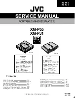
background image

SERVICE MANUAL

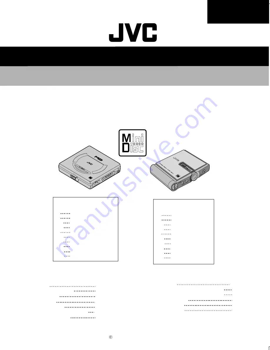
PORTABLE MINIDISC PLAYER 

No.20738

Jan. 1999

COPYRIGHT    1999 VICTOR COMPANY OF JAPAN, LTD.

Printed in Japan
9901  (V )

VICTOR COMPANY OF JAPAN, LIMITED

AUDIO DIVISION,10-1,1Chome,Ohwatari-machi,Maebashi-city,371-8543,Japan

XM-P55
XM-PJ1

(No.20738)

XM-P55
XM-PJ1

XM-P55
XM-PJ1

Contents

Safety Precautions
Instructions (For XM-P55&PJ1)    
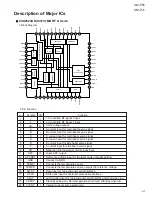
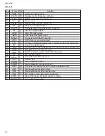
Description of Major ICs 
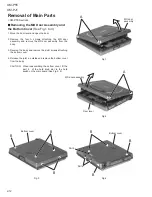
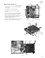
Removal of Main Parts         
Maintenance of MD Pickup 
Procedures of Changing the MD Pickup
Self-diagnosis Function of MD

Block Diagrams 
Standard Schematic Diagrams (XM-P55)
Standard Schematic Diagrams (XM-PJ1)
Printed Circuit Boards
Parts List (XM-P55)
Parts List (XM-PJ1)

1-2
1-3~16
2-1
2-12
2-23
2-23
2-24

2-27
2-29
2-36
2-42,43
3-1~15
4-1~15

B
E
EE
EN
J
UB
US
UT
UX
UY

Area Suffix 

 (XM-PJ1 )

U.K. (BU)
Continental Europe (BU)
Russian Federation (BU)
Northern Europe (BU)
U.S.A. (BU)
Hong kong (BU,GD)
Singapore (BU)
Taiwan (BU)
Saudi Arabia (BU)
Argentina (BU)

Area Suffix 

B
E
EE
EN
J
UB
US
UT
UX
UY

 (XM-P55 )

U.K. (BU,SL)
Continental Europe (BU,SL)
Russian Federation (BU,SL)
Northern Europe (BU,SL)
U.S.A. (SL)
Hong kong (BU,GN,SL)
Singapore (BU,SL)
Taiwan (SL)
Saudi Arabia (SL)
Argentina (SL)

OPEN

X

M

- P

5

5

XM-P55

XM-PJ1

Summary of Contents for XM-P55

Page 1: ...hematic Diagrams XM PJ1 Printed Circuit Boards Parts List XM P55 Parts List XM PJ1 1 2 1 3 16 2 1 2 12 2 23 2 23 2 24 2 27 2 29 2 36 2 42 43 3 1 15 4 1 15 B E EE EN J UB US UT UX UY Area Suffix XM PJ1 U K BU Continental Europe BU Russian Federation BU Northern Europe BU U S A BU Hong kong BU GD Singapore BU Taiwan BU Saudi Arabia BU Argentina BU Area Suffix B E EE EN J UB US UT UX UY XM P55 U K BU...

Page 2: ...may be left over on some parts of the chassis Therefore pay attention to such burrs in the case of preforming repair of this system Safety Precaution Please use enough caution not to see the beam directly or touch it in case of an adjustment or operation check ...

Page 3: ... input for main beam servo signal B current input for main beam servo signal C current input for main beam servo signal D current input for main beam servo signal E current input for side beam servo signal F current input for side beam servo signal Reflection light quantity monitor signal input Laser APC output Reference voltage input for the laser power intensity setting Connect to GND Connects t...

Page 4: ...output Reflection light quantity signal output for the main beam servo detector RF ABCD bottom hold signal output Peak hold signal output for the RF ABCD signals RF equalizer output Connects the RFAGC capacitor RFAGC input User comparator output User comparator non inverted input Connects the capacitor for ADIP amplifier feedback circuit User operational amplifier output User operational amplifier...

Page 5: ...ND FC FG2 FG RESET CLOCK SLOPE OSC VS WF VF UF COMF CPOUT CPC2 CP2 CPC1 CP1 VCO RMAX RMIN VCOIN VCC MCLOCK S S BRAKE VCONT VCREF Voltage Driver Power Stage Level Shifter Charge Pump VCO Sensorless Logic Phase Comparator 1 8 Timing Controllor PWM F R Controllor Full Wave Rectifier Sample and Hold 1 Pin Layout 2 Block Diagram ...

Page 6: ...ation frequency Setting of VCO maximum oscillation frequency Setting of VCO minimum oscillation frequency Forms motor waveform Forms motor waveform Forms motor waveform Forms motor waveform VCO oscillation frequency control Monitors CLOCK signal Ground of circuits except for output section Sample board for output current detection Forms saw tooth wave for PWM wave formation Forms santooth waveform...

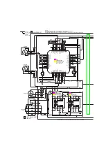
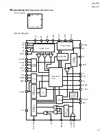
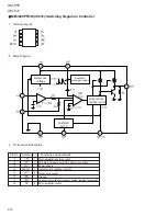
Page 7: ...XM P55 XM PJ1 2 5 CXD2655R IC351 Digital Servo Processor Block Diagram ...

Page 8: ...for master PLL of playback digital PLL Filter output for master PLL of playback digital PLL Peak hold signal input for quantity of light Bottom hold signal input for quantity of light Signal input for quantity of light Focus error signal input Auxiliary input 1 Center voltage input Monitor output of A D converter input signal Analog power supply Analog ground Sled error signal input Tracking error...

Page 9: ...ntroller Port 1 Port 9 Clock generator Port 4 Interrupt controller ROM Mask ROM PROM Flash memory 16 bits integrated timer unit ITU DMA controller DMAC Refresh controller Watch dog timer WDT Serial communication interface SCI 2ch Programmable timing pattern controller TPC A D converter D A converter RAM Terminal Layout Block Diagram Port B Port A Port 7 ...

Page 10: ...NT3 terminal of CXD2655R Connect to SENS terminal of CXD2655R EEPROM communication serial data input Non connection ACTIVE CLEAR BASS circuit ON OFF output Power supply Non connection Non connection Connect to XRST terminal of CXD2655R Connect to XLAT terminal of CXD2655R Supplies 12V when flash memory is writing Ground Remote control UART output Connect to SWDT terminal of CXD2655R Remote control...

Page 11: ...river power supply Driver output Power ground Driver output Driver power supply CH 1 control signal input CH 1 control signal input CH 2 control signal input CH 2 control signal input CH 4 control signal input CH 4 control signal input CH 3 control signal input CH 3 control signal input Driver output Driver output Power ground Power ground Driver power supply Driver power supply Driver output Powe...

Page 12: ...Soft start S C P Output drive control circuit Santooth wave generator Pin No Symbol Functions and operations Error amplifier inversion input Soft start capacity for SCP setting connection Power supply Output current setting control Totem pole output Ground Capacity for oscillation frequency setting resistant connection Error amplifier output ...

Page 13: ...abling input Output enabling input Data input Power supply 3 3V Power supply 0V Non connection OE DQ0 DQ3 WE RAS CAS 10 0 VSS VDD 0 10 0 10 Row Address Buffer Column Address Buffer On Chip VBB Generator CBR Refresh Counter Row Decoder Word Driver Memory Cell Sense Amp Column Decoder I O Selector Data Output Buffer Data Input Buffer Write Clock Generator Clock Generator ...

Page 14: ...assembly from the body Reverse the body and remove the six B screws attaching the bottom cover Release the joint a outside and remove the bottom cover from the body CAUTION When reassembling the bottom cover fit the part b of the hold knob slot to the hold switch on the main board See Fig 4 5 Fig 1 Fig 2 Fig 4 Fig 3 MD door assembly MD door assembly Bottom cover Part a Part b Bottom cover A Door l...

Page 15: ...embly while pulling the cabinet assembly of the headphone jack outwards Move the main board in the direction of the arrow in Fig 6 and remove it upward from the two parts d of the bending on the flame assembly Disconnect the flexible harnesses from connector CN300 and CN401 on the reverse side of the main board Fig 5 Fig 6 Fig 7 Hold switch Main board Part c unsoldering Main board Headphone jack a...

Page 16: ...PJ1 2 14 Removing the Mechanism Assembly See Fig 8 1 Remove the two E screws attaching the mechanism assembly and remove the mechanism assembly from the flame assembly Fig 8 Mechanism assembly E E Flame assembly ...

Page 17: ...ng the bottom cover on the side of the body Remove the bottom cover from the body while releasing the tab a of the bottom cover on the side of the hold switch to the inside 1 2 3 4 CAUTION When reassembling make sure that the convexity of the hold switch is fitted to the concave of the switch knob before inserting the tab a of the bottom cover assembly Battery lid Bottom cover assembly B A A Botto...

Page 18: ...mbly Remove the screw D attaching the cabinet on the upper side of the body Reverse the body and remove the two E screws attaching the cabinet on the back of the body Release the two joints b on the flame assembly side of the battery case in the direction of the arrow and remove the cabinet from the flame assembly Unsolder the two harnesses one is orange the other is gray connected to the main boa...

Page 19: ...rd Move the main board to the inside and remove it upward while releasing it from the two hinges f on the bending of the flame assembly Disconnect the flexible harnesses from connector CN300 and CN401 on the reverse side of the main board 1 2 3 4 5 6 7 CAUTION When reattaching the flexible harness 1 position it to the six g points and fix it with a double sided tape See Fig 10 Fig 9 Fig 10 Fig 11 ...

Page 20: ...er 1 2 3 4 5 CAUTION When reattaching the flexible harness 1 position it to the six g points and fix it with a double sided tape See Fig 10 Removing the Mechanism Assembly See Fig 14 Remove the bottom cover Remove the front cover Remove the cabinet Remove the main board Remove the two H screws attaching the mechanism assembly and remove the mechanism assembly from the flame assembly 1 2 3 4 5 Fig ...

Page 21: ...t the holder assembly from the shaft of the chassis assembly CAUTION When reassembling first attach the part b of the holder assembly to the shaft of the chassis assembly Next attach the U shaped notch to the shaft Removing the Spindle Motor See Fig 3 1 2 Unsolder the part c of the flexible harness connected to the spindle motor Remove the three A screws attaching the spindle motor and remove the ...

Page 22: ... the other side Remove the spacer of the flexible harness extending from the pickup unit marked d and remove the pickup unit from the chassis assembly Removing the Pickup See Fig 5 6 1 2 Remove the screw C from the pickup unit and the lead spring Pull out the main shaft from the pickup B Fig 4 Fig 5 Chassis assembly d Hold spring Slit washer Worm gear Part e Hold spring Pickup unit Shaft Guide bas...

Page 23: ...pacer to the folded flexible harness and fix the flexible harness to the chassis assembly see Fig 7 8 Attach a spacer between the chassis boss and the flexible harness see Fig 9 Make sure that the flexible harness is folded fast and fixed to the right position Reassembling the Pickup Unit Fig 8 Fold fast Attach a spacer Fix fast not to unfold Fold fast Attach a spacer Chassis assembly Attach a spa...

Page 24: ...harnesses extending from the feed motor Remove the screw D attaching the feed motor then the spring Remove the feed motor from the feed motor base Lift the feed motor base and pull out the screw shaft assembly Fig 10 Feed motor base Soldering Feed motor Wheel gear Shaft base Screw shaft gear Spring D D ...

Page 25: ...the resistors Since the service life of the laser diode will be exhausted when the laser power is low it is necessary to change the pickup Meanwhile do not pickup Otherwise the pickup will be damaged due to over current 3 Method of measuring the drive current of laser diode When the voltage measured at the both side of carbon resistor R301 on the MD servo P C board VMW2424A have become 45mV or ove...

Page 26: ... into the self diagnosis mode and the self diagnosis starts Test s Command for the self diagnosis mode 00 Wait to Test command DD Going to Resume s EEPROM initialize DE Going to servo s EEPROM initialize E2 Turn on the leaser of PLAY D3 Turn up the laser D4 Turn down the laser D1 Turn off the laser D5 Rewind to the FEED D6 Adjust to the PRE DISC D7 Adjust to the MO DISC 92 Break out the trouble Th...

Page 27: ...s Except to recieve DF DD Recieve DF 00 Recieve DF 00 Recieve DF 00 Recieve DF 00 Recieve DF 00 Recieve DF 00 Recieve DF 00 Recieve DF D1 Recieve DF 00 XX YY Recieve DF 00 XX YY Recieve DF 00 Issue to DB Issue to DE Issue to DF Issue to DF Issue to D1 Issue to D4 01 Issue to D3 01 Issue to E2 Issue to DE Issue to DE Issue to DE Initial to resume Initial to the servo Push to BASS Push to BASS Push ...

Page 28: ... Except to recieve DF D5 Recieve time out at 200ms Except to recieve DF 00 Recieve time out at 200ms Except to recieve DF 00 Recieve time out at 200ms Except to recieve DF 00 Issue to D5 Issue to DF Issue to DF Issue to DF Issue to D6 Issue to D7 Processor Processor Processor Receive DF D5 Receive DF 00 Receive DF 00 Receive DF 00 Receive DF D6 Receive DF D7 OK OK OK Lock to display at 2sec Lock t...

Page 29: ... 2 27 Block Diagrams RF IC DSP 16M D RAM PICKUP DRIVER DRIVER SLED SPINDLE Audio POWER SUPPLY HP JACK CNT Micro computer ACB BEEP MUTE REMOTE CONTROL Each Block LEVEL DIAGRAM ACB Circuit Headphone AMP Servo FCS TRK ...

Page 30: ...XM P55 XM PJ1 2 28 MEMO ...

Page 31: ...A B C D 1 2 3 4 5 XM P55 XM PJ1 2 29 XM P55 Except to U S A BLOCK C BLOCK D BLOCK A BLOCK B Standard Schematic Diagrams ...

Page 32: ...A B C D 1 2 3 4 5 XM P55 XM PJ1 2 30 Digital signal To BLOCK B To BLOCK C XM P55 Except to U S A BLOCK A ...

Page 33: ...A B C D 1 2 3 4 5 XM P55 XM PJ1 2 31 Digital signal Analogue signal BLOCK B To BLOCK A To BLOCK D XM P55 Except to U S A ...

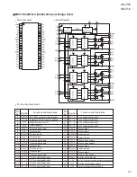
Page 34: ...A B C D 1 2 3 4 5 XM P55 XM PJ1 2 32 To BLOCK D To BLOCK A BLOCK C XM P55 Except to U S A ...

Page 35: ...A B C D 1 2 3 4 5 XM P55 XM PJ1 2 33 To BLOCK B BLOCK D XM P55 Except to U S A To BLOCK C ...

Page 36: ...XM P55 XM PJ1 2 34 MEMO ...

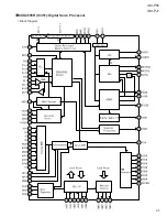
Page 37: ...A B C D E F G 2 35 XM P55 XM PJ1 2 9 2 9 2 9 Ý P55J ONLY ...

Page 38: ...H B C D E F G 2 36 XM P55 XM PJ1 2 10 2 10 2 10 Ý D BLOCK C BLOCK o U S A Digital signal BLOCK A To BLOCK B To BLOCK C XM PJ1 Except to U S A ...

Page 39: ...A B C D 1 2 3 4 5 XM P55 XM PJ1 2 37 BLOCK B XM PJ1 Except to U S A To BLOCK C To BLOCK A Digital signal Anologue signal ...

Page 40: ...A B C D 1 2 3 4 5 XM P55 XM PJ1 2 38 To BLOCK A To BLOCK D BLOCK C XM PJ1 Except to U S A ...

Page 41: ...A B C D 1 2 3 4 5 XM P55 XM PJ1 2 39 To BLOCK C To BLOCK B BLOCK D XM PJ1 Except to U S A ...

Page 42: ...XM P55 XM PJ1 2 40 MEMO ...

Page 43: ...A B C D E F G 2 41 XM P55 XM PJ1 2 9 2 9 2 9 Ý XM PJ1 J ONLY ...

Page 44: ...H B C D E F G 2 42 XM P55 XM PJ1 ard Parts side Block No XM P55 ONLY Circuit Boards 2 10 2 10 2 10 Ý Solder side chip parts ...

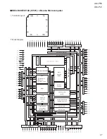
Page 45: ...A B C D 1 2 3 4 5 XM P55 XM PJ1 2 43 Block No Block No Headphone Jack Board Switch Board ...

Page 46: ...XM P55 XM PJ1 2 44 MEMO ...

Page 47: ...U SL Northern Europe BU SL U S A SL Hong kong BU GN SL Singapore BU SL Taiwan SL Saudi Arabia SL Argentina SL Contents Exploded View of General Assembly and Parts List 3 2 MD Mechanism Ass y and Parts List 3 4 Electrical Parts List 3 6 Packing Materials and Accessories Parts List J 3 10 Packing Materials and Accessories Parts List E EE EN 3 12 Packing Materials and Accessories Parts List B UB US U...

Page 48: ...A B C D 1 2 3 4 5 XM P55 XM PJ1 3 2 Block No 44 General Exploded View and Parts List MODEL XM P55 ...

Page 49: ...XM P55 XM PJ1 3 3 ...

Page 50: ...A B C D 1 2 3 4 5 XM P55 XM PJ1 3 4 MD Mechanism Ass y and Parts List Block No MODEL PPM ...

Page 51: ...XM P55 XM PJ1 3 5 ...

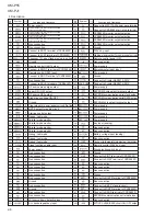
Page 52: ...XM P55 XM PJ1 3 6 Electrical Parts List Main board ...

Page 53: ...XM P55 XM PJ1 3 7 ...

Page 54: ...XM P55 XM PJ1 3 8 ...

Page 55: ...XM P55 XM PJ1 3 9 Headphone Jack board Switch board ...

Page 56: ...A B C D 1 2 3 4 5 XM P55 XM PJ1 3 10 Packing Materials and Accessories Parts List Block No Block No J Version Section turn up turn down ...

Page 57: ...XM P55 XM PJ1 3 11 Packing Parts list Accessories Parts list ...

Page 58: ...A B C D 1 2 3 4 5 XM P55 XM PJ1 3 12 Packing Materials and Accessories Parts List Block No Block No E EE EN Version Section turn up turn down ...

Page 59: ...XM P55 XM PJ1 3 13 Packing Parts list Accessories Parts list ...

Page 60: ...A B C D 1 2 3 4 5 XM P55 XM PJ1 3 14 Packing Materials and Accessories Parts List Block No Block No B UB US UT UX UY Version Section turn up turn down ...

Page 61: ...XM P55 XM PJ1 3 15 Packing Parts list Accessories Parts list ...

Page 62: ...XM P55 XM PJ1 3 16 MEMO ...

Page 63: ...n BU Northern Europe BU U S A BU Hong kong BU GD Singapore BU Taiwan BU Saudi Arabia BU Argentina BU Contents Exploded View of General Assembly and Parts List 4 2 MD Mechanism Ass y and Parts List 4 4 Electrical Parts List 4 5 Packing Materials and Accessories Parts List J 4 10 Packing Materials and Accessories Parts List E EE EN 4 12 Packing Materials and Accessories Parts List B UB US UT UX UY 4...

Page 64: ...A B C D 1 2 3 4 5 XM P55 XM PJ1 4 2 C991 J991 Block No General Exploded View and Parts List MODEL XM PJ1 ...

Page 65: ...XM P55 XM PJ1 4 3 ...

Page 66: ...XM P55 XM PJ1 4 4 Block No MD Mechanism Exploded View and Parts List MD Mechanism as same as XM P55 Please refer of the page 3 4 and 3 5 ...

Page 67: ...XM P55 XM PJ1 4 5 Electrical Parts List Main board ...

Page 68: ...XM P55 XM PJ1 4 6 ...

Page 69: ...XM P55 XM PJ1 4 7 ...

Page 70: ...XM P55 XM PJ1 4 8 ...

Page 71: ...XM P55 XM PJ1 4 9 Headphone Jack board Switch board ...

Page 72: ...A B C D 1 2 3 4 5 XM P55 XM PJ1 4 10 Packing Materials and Accessories Parts List Block No Block No J Version Section turn up turn down ...

Page 73: ...XM P55 XM PJ1 4 11 Packing Parts list Accessories Parts list ...

Page 74: ...A B C D 1 2 3 4 5 XM P55 XM PJ1 4 12 Packing Materials and Accessories Parts List Block No Block No E EE EN Version Section turn up turn down ...

Page 75: ...XM P55 XM PJ1 4 13 Packing Parts list Accessories Parts list ...

Page 76: ...A B C D 1 2 3 4 5 XM P55 XM PJ1 4 14 Packing Materials and Accessories Parts List Block No Block No A1 A4 B UB US UT UX UY Version Section turn up turn down ...

Page 77: ...XM P55 XM PJ1 Packing Parts List Accessories Parts List ...

Page 78: ...Printed in Japan 9901 V VICTOR COMPANY OF JAPAN LIMITED AUDIO DIVISION 10 1 1Chome Ohwatari machi Maebashi city 371 8543 Japan No 20738 XM P55 XM PJ1 ...

Reviews: