background image


PT568 Service Manual


1


Dangerous! 


Do not connect the AC power or DC power over 8.6V with 

any connector or terminal of the radio. Otherwise it will cause fire, 

electric shock or damage to the radio. 


Warning! 


Do not reverse power connection. 

It may cause harm to the radio if signal input on the antenna 

connector is higher than 20 dBm (100mW). 

Do not turn on the radio before the antenna or load connection 

is completed. 

If the antenna has been damaged, do not use the radio. 

Damaged antenna may cause light burning on skin. 

Though the radio is waterproof, it's better to avoid putting it in 

rain or snow, or any other liquid to ensure its life and 

performance. 


Statement! 


Kirisun Electronics (Shenzhen) Co., Ltd owns the copyright of 

KSP568 software. 

Unauthorized Duplication of KSP568 software is strictly 

prohibited. 

Kirisun Electronics (Shenzhen) Co., Ltd owns the copyright of 

the MCU software code. 

Kirisun Electronics (Shenzhen) Co., Ltd owns the copyright of 

the radio outward appearance/structure/circuit design. 

Kirisun Electronics (Shenzhen) Co., Ltd owns the copyright of 

this service manual. Unauthorized publication is prohibited. 

Kirisun Electronics (Shenzhen) Co., Ltd owns the trademarks 

“KIRISUN”,

 “

”, “

”, and “

科立讯

”. 


Content 


Chapter 1 Overview ................................................................... 2 

Chapter 2 External View and Functional Keys........................... 2 

Chapter 3 Circuit Description..................................................... 3 

Chapter 4 Mode Introduction ..................................................... 8 

Chapter 5 Disassembly for Repair............................................ 11 

Chapter 6 Adjustment............................................................... 12 

Chapter 7 Specifications........................................................... 15 

Chapter 8 Troubleshooting ....................................................... 15 

Chapter 9 KBC-70Q Charger ................................................... 17 

Appendix 1 Abbreviations........................................................ 18 

Appendix 2 Electronic Parts List.............................................. 18 

Appendix 3 Structural Parts List .............................................. 22 

Appendix 4 Accessories ........................................................... 23 

Figure 1 PT568 Block Diagram................................................ 24 

Figure 2 PT568 Schematic Circuit Diagram............................. 25 

Figure 3 PT568 Top Layer Position Mark Diagram ................. 26 

Figure 4 PT568 Bottom Layer Position Mark Diagram ........... 27 

Figure 5 PT568 Top Layer Position Value Diagram................. 28 

Figure 6 PT568 Bottom Layer Position Value Diagram ........... 29 


Summary of Contents for PT568-01

Page 1: ...ns the copyright of the MCU software code Kirisun Electronics Shenzhen Co Ltd owns the copyright of the radio outward appearance structure circuit design Kirisun Electronics Shenzhen Co Ltd owns the copyright of this service manual Unauthorized publication is prohibited Kirisun Electronics Shenzhen Co Ltd owns the trademarks KIRISUN and 科立讯 Content Chapter 1 Overview 2 Chapter 2 External View and ...

Page 2: ...ded to avoid using radios in a car that is moving as the radio wave might interfere the auto engine and cause it to stop working Replacement Parts All components used for repair should be supplied by Kirisun Components of the same type available on the market are not surely able to be used in this product and we do not guarantee the quality of the product using such components If you want to apply...

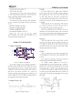
Page 3: ...eceiver RX Figure 3 2 Principle of Receiver Front end The signal coming from the antenna passes through the RX TX switch circuit D1 D2 D4 and D5 and passes through a BPF comprises of C37 C227 L8 L15 C70 C126 D30 C218 L9 C230 C128 D26 C217 L10 C229 C127 and D24 to remove unwanted out of band signal and is sent to the low noise amplifier LNA consists of Q20 and its peripheral components to be amplif...

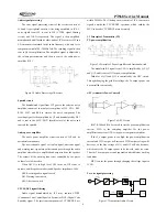
Page 4: ...ns on IC8 starts to operate and the speaker makes sound Speaker impedance 16Ω Q38 Receiving audio signal switch Q51 Warning tone switch Q25 Alert tone switch CTCSS DCS signal filtering Audio signal demodulated by IC5 may contain CTCSS Continuous Tone Control Squelch System or DCS Digital Code Squelch signal The spectrum components of CTCSS DCS are within 2 250Hz The filtering circuit consists of I...

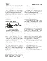
Page 5: ...nd is then compared with the reference frequency to obtain error signal The signal is then filtered by a low pass filter and is sent to VCO to change the oscillation frequency of the VCO enabling the frequency to reach the set value Then the VCO is locked N FVCO FR N Times of frequency division FVCO Oscillation frequency of VCO FR Reference frequency Unlock detection When PLL is unlocked Pin 14 of...

Page 6: ...er and is guided by a continuous sub audio signal If CTCSS is set the communication between the transmitting and receiving radios can be realized only when the two radios have set the same CTCSS frequency In doing this disturbance from other signals can be avoided PT568 has 39 groups of standard CTCSS frequencies for your selection See table 3 1 The CTCSS signal is generated by MCU and is passed t...

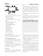
Page 7: ... O Clock of voice annunciation IC 37 RLED P63 O Red LED control H On 38 NC P07 I A D0 Connect the pull up resistor with VCC and connect the pull down resistor with VSS 39 NC NC 40 NC NC 41 TI P06 I A D1 QT DQT signal input 42 BUSY P05 I A D2 Busy signal input 43 BATT P04 I A D3 Battery voltage detect 44 VREF I Connect with VCC 45 SAVE P60 O Battery saving control H supply power L power saving 46 M...

Page 8: ...wer Guarantee attenuation 35 0db or higher Terminal impedance 2 0kΩ Table 3 8 Schematic Diagram for Packaging of Semiconductor Devices 3SK318 M YB G1 G2 D S G S D C C C C B B B B E E E E G D S 2SK1824 Mark B1 2SC5108 M MC C B E M R24 2SC3356 C B E 2SC4617 C B E C B E 2SC4738 KTC4082 C B E 2SC1623 M L6 KTA1298 DTC144EE M 16 GND IN OUT HT7150 1 RD01MUS1 D G S S RD07MVS1 RDA0002 1 2 3 DA221 M K 2SK30...

Page 9: ...delete the nuisance channel temporarily 8 High Low Power Switch Press the preprogrammed High Low Power Switch button to switch between high and low transmitting power of the radio 9 Momentary Monitor Press and hold the preprogrammed Momentary Monitor button to disable CTCSS DCS signalling and release the button to resume normal operation 10 Monitor Press the preprogrammed Monitor button to disable...

Page 10: ... Wideband 9 Five frequency points for SQL1 Off Wideband 10 Five frequency points for SQL1 On Narrowband 11 Five frequency points for SQL1 Off Narrowband 12 Five frequency points for QT 67 0Hz Deviation Wideband 13 Center frequency point for QT 67 0Hz Deviation Narrowband 14 Five frequency points for QT 151 4Hz Deviation Wideband 15 Center frequency point for QT 151 4Hz Deviation Narrowband 16 Five...

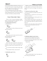
Page 11: ...s body Note Do not short circuit the battery terminals or dispose battery in fire Do not disassemble the battery casing by yourself 5 2 Installing Removing the belt clip Match the two holes of the belt clip with those on the rear of the radio and then fix the belt clip to the radio using the two supplied 2 5 8 0 screws Loose the fixing screws to remove the belt clip 5 3 Removing the chassis from t...

Page 12: ...ure all equipment has been well connected to the ground Before test adjustment make sure the antenna output terminal has been correctly connected to corresponding equipment or load The transmitter output terminal must be terminated with an RF power attenuator and connected to a standard signal generator SSG frequency counter deviation meter spectrum analyzer Make sure no transmission operation is ...

Page 13: ...MHz 445 125MHz 469 975MHz 6 3 2 PLL frequency 1 In the Tuning Mode double click 6250Hz precision to enter Adjust the parameter among 0 255 to make the Tx frequency at the rated value error within 200Hz 2 In the Tuning Mode double click 2500Hz precision to enter Adjust the parameter among 0 255 to make the Tx frequency at the rated value error within 200Hz 6 3 3 Tx Power In the Tuning Mode double c...

Page 14: ...e RF signal frequency of the test equipment to be the same with the receiving frequency of that frequency point and adjust the signal level to be 118dBm Then adjust the frequency of the modulation signal to be 1kHz and the deviation to be 3kHz The programming software will adjust the value automatically When the value keeps stable the adjustment of that frequency point is completed Then click the ...

Page 15: ...5 kHz N 12 5kHz Operating Temperature 25 55 Antenna Impedance 50Ω Frequency Stability 2 5ppm Battery Standard Configuration Li Poly Battery 1500mAH 7 4V Dimension W H D 52 5mm 111mm 33 5mm Weight 270g with antenna and 1500mAh Li Poly Battery 7 2 Receiver Section Sensitivity 12dB SINAD 0 25μV W 0 28μV N Adjacent Channel Selectivity W 70dB N 60dB Intermodulation Interference 65dB Audio Output Power ...

Page 16: ...nt charger which is safe and reliable and has fast charging speed and high charging saturation 2 Status indication function In the pre charge process the red LED will flash in the charging process the red LED will light if the radio is fully charged or no battery is inserted to the charger slot or the battery is in the protection status the green LED will light if the battery output is in short ci...

Page 17: ...r amplifier TDA8541 SO8 ROHS pcs 1 IC8 7 102 HT7130 R01 Voltage regulator IC HT7130 1 SOT 89 ROHS pcs 1 IC14 8 102 HT7150 R01 Voltage regulator IC HT7150 1 ROHS pcs 1 IC12 9 102 M2902V R01 Operational amplifier NJM2902V OP AMP ROHS pcs 3 IC4 IC6 IC7 10 102 M2904V R01 Operational amplifier NJM2904V OP AMP ROHS pcs 1 IC3 11 103 00MA77 R01 Chip HF switch diode MA77 0805 ROHS pcs 1 D1 12 103 1SR154 R0...

Page 18: ...s 1 CF1 52 108 XF5165 R01 Chip crystal filter DSF753SBF 51 65MHz 4kHz 3dB 7 0x5 0x1 3 mm ROHS pcs 1 XF1 53 109 040000 R01 Chip resistor 0402 0R 5 ROHS pcs 20 C67 C166 C250 R7 R18 R24 R27 R30 R141 R182 R183 R203 R217 R241 R260 R261 R262 R268 R278 R283 54 109 040100 R01 Chip resistor 0402 10R 5 ROHS pcs 6 R95 R96 R98 R101 R127 R200 55 109 040101 R01 Chip resistor 0402 100R 5 ROHS pcs 6 R4 R12 R89 R9...

Page 19: ...2 5 6K 5 ROHS pcs 9 R61 R62 R63 R64 R65 R132 R184 R195 R302 96 109 040563 R01 Chip resistor 0402 56K 5 ROHS pcs 12 R16 R173 R175 R176 R177 R178 R225 R239 R254 R267 R270 R284 97 109 040564 R01 Chip resistor 0402 560K 5 ROHS pcs 1 R163 98 109 040682 R01 Chip resistor 0402 6 8K 5 ROHS pcs 2 C276 R220 99 109 040683 R01 Chip resistor 0402 68K 5 ROHS pcs 1 R245 100 109 040684 R01 Chip resistor 0402 680K...

Page 20: ...pacitor 0402 2P 0 25P 50V C0G ROHS pcs 2 C218 C301 142 112 043300 R01 Chip capacitor 0402 30P 5 50V C0G ROHS pcs 2 C200 C319 143 112 043330 R01 Chip capacitor 0402 33P 5 50V C0G ROHS pcs 1 C171 144 112 043333 R01 Chip capacitor 0402 0 033uF 10 16V X7R ROHS pcs 3 C213 C223 C283 145 112 043360 R01 Chip capacitor 0402 36P 5 50V C0G ROHS pcs 1 C90 146 112 043392 R01 Chip capacitor 0402 3900P 10 50V X7...

Page 21: ... R02 Chip capacitor 0805 330nF 10 16V X7R ROHS pcs 2 C33 C209 189 112 102104 R01 Chip Ta capacitor TS model SIZE A 0 1uF 20 35V ROHS pcs 2 C193 C204 190 112 102106 R02 Chip Ta capacitor TS model SIZE A 10uF 20 10V ROHS pcs 3 C197 C203 C210 191 112 102156 R01 Chip Ta capacitor TS model SIZE A 15uF 20 6 3V ROHS pcs 1 C208 192 112 102225 R01 Chip Ta capacitor TS model SIZE A 2 2uF 20 10V ROHS pcs 1 C...

Page 22: ...s 1 4 201 000568 R04B PT568 Top Cover PC ABS black ROHS pcs 1 5 201 000568 R05C PT568 PTT Cover PC ABS black ROHS pcs 1 6 201 000568 R06A PT568 Volume Knob ABS black ROHS pcs 1 7 201 000568 R07A PT568 Channel Selector Knob ABS black ROHS pcs 1 8 201 000568 R09A PT568 Light Guide PC transparent ROHS pcs 1 9 201 000568 R10B PT568 Earphone Jack Cover TPU black hardness 90 ROHS pcs 1 10 201 000568 R11...

Page 23: ...ed Adhesive Tape for Front Casing 3M double sided adhesive tape white 18 2mm ROHS pcs 2 33 301 20040G R01B Screw M2 0 4 0 pan plus Ni plated ROHS pcs 13 For fixing PCB board and antenna connector 34 301 20080G R02B Screw M2 0 8 0 pan torx Ni plated ROHS pcs 2 For fixing Al alloy chassis 35 301 25080J R01 Screw M2 5 8 0 pan plus black Zn plated ROHS pcs 2 For fixing top cover or belt clip Appendix ...

Page 24: ...1136 NOISE DET BUSY SIGNEL TO MCU AF AMP 5R AF AMP QT DQT OUT TO MCU AF AMP AF AMP 5R 5R 5R AF POWER AMP AF MUTE MUTE 1 2 3 4 5 W558 CLK FROM MCU DATA FROM MCU BUSY TO MCU W N AF MUTE MUTE 5M DTMF BEEP FROM MCU AF AMP 5C GND AF POWER AFCN POWER SW 3 3 4 4 2 2 1 1 2 SP K JACK TXD 1 M IC JACK AF AMP 5C W N GND GND RXD DTMF BEEP FROM MCU MODE MCU R5F212A8 7 3MHz RESET EEPROM 5M 5M 5M ENCODER KEYS TOP...

Page 25: ...C 46 4 7 u F 1 6V C 45 471 C 48 471 K 4 PFI R 80 10K C 49 471 D 20 G R EEN D 19 1 2 3 4 5 6 SW2 EN C O D ER Q 34 D TA 144EE L19 B LM11A 221 S SW1 PO W V O L C 67 0R C 76 C 7 7 C 78 9P C 79 103 C 80 474 C 81 C 152 471 T 1 PD Q 36 2SK 1824 C 276 6 8K R 157 1K R 247 100K C 278 102 R 158 100K R 239 56K R 243 100K C 281 C31 471 R 250 L44 BLM11A 221 S VC 1 GND 2 VCC 4 OUT 3 X 4 12 8MH z R 257 100K C 289...

Page 26: ......

Page 27: ......

Page 28: ...PT568 Service Manual 28 Figure 5 PT568 Top Layer Position Value Diagram ...

Page 29: ...PT568 Service Manual 29 Figure 6 PT568 Bottom Layer Position Value Diagram ...

Reviews: