background image

SERVICE MANUAL

SERVICE MANUAL

CAUTION

BEFORE SERVICING THE UNIT, READ THE “SAFETY PRECAUTIONS”
IN THIS MANUAL.

Internal Use Only

Mini Hi-Fi AUDIO

APRIL

, 2016

P/NO : 

AFN77

483239

MODEL: OM7560

MODEL: OM7560

Summary of Contents for OM7560

Page 1: ...SERVICE MANUAL SERVICE MANUAL CAUTION BEFORE SERVICING THE UNIT READ THE SAFETY PRECAUTIONS IN THIS MANUAL Internal Use Only Mini Hi Fi AUDIO APRIL 2016 P NO AFN77483239 MODEL OM7560 MODEL OM7560 ...

Page 2: ...CONTENTS SECTION 1 GENERAL SECTION 2 CABINET MAIN CHASSIS SECTION 3 ELECTRICAL SECTION 4 MECHANISM DM19AC SECTION 5 REPLACEMENT PARTS LIST 1 1 ...

Page 3: ...SECTION 1 SUMMARY CONTENTS SERVICING PRECAUTIONS 1 3 ESD PRECAUTIONS 1 5 HIDDEN KEY MODE 1 6 SERVICE INFORMATION FOR EEPROM 1 7 PROGRAM DOWNLOAD GUIDE 1 8 SPECIFICATIONS 1 11 1 2 ...

Page 4: ...age the eyes Absolutely never permit laser beams to enter the eyes Also NEVER switch ON the power to the laser output part lens etc of the pick up if it is damaged 5 Cleaning the lens surface If there is dust on the lens surface the dust should be cleaned away by using an air bush such as used for camera lens The lens is held by a delicate spring When cleaning the lens surface therefore a cot ton ...

Page 5: ... replacing a component part first disconnect the power supply lead wire from the unit 2 All equipment measuring instruments and tools must be grounded 3 The workbench should be covered with a conductive sheet and grounded When removing the laser pick up from its conductive bag do not place the pick up on the bag This is because there is the possibility of damage by static electricity 4 To prevent ...

Page 6: ...t to damage ESD devices 5 Do not use freon propelled chemicals These can generate electrical charges sufficient to damage ESD devices 6 Do not remove a replacement ESD device from its protective package until immediately before you are ready to install it Most replacement ESD devices are packaged with leads electrically shorted together by conductive foam aluminum foil or comparable conductive mat...

Page 7: ...on code Front Key STOP RCU Key PLAY PAUSE You can change Audio MCU Version CD Controller Version EEPROM Option by SKIP 3 Clear EEPROM Front Key STOP RCU Key SKIP CD Model 0 DVD Model 4 Edit EEPROM Front Key STOP RCU Key SKIP You can change the digit of option by SKIP You can edit 0 f by REPEAT or PLAY PAUSE key 5 Measure Mode Bypass Front Key STOP RCU Key 8 HW output measure ...

Page 8: ...oo This is an example Front Stop Remote control push same timing during 5 s FLD OP00 Move to appropriate position And make changes with remote control REPEAT key Press Stop Key VFD WRITE OK Front Stop Remote control push same timing during 5 s VFD E2P CLR Completed 1 7 SERVICE INFORMATION FOR EEPROM ...

Page 9: ...ng file proceeds in the same way at USB1 function and USB2 function Caution When downloading the file you should neither unplug the USB device change to the other function nor power off the device USB device must be unplugged when the downloading process is completed ON VFD DISPLAY SCREEN 1 Fast Format USB device 2 Copy Firmware file to USB device NO USB Insert USB device at USB function SEARCH MI...

Page 10: ... Downloading file proceeds in the same way at USB1 function and USB2 function Caution When downloading the file you should neither unplug the USB device change to the other function nor power off the device USB device must be unplugged when the downloading process is completed ON VFD DISPLAY SCREEN 1 Fast Format USB device 2 Copy Firmware file to USB device NO USB Insert USB device at USB function...

Page 11: ...oading file proceeds in the same way at USB1 function and USB2 function Caution When downloading the file you should neither unplug the USB device change to the other function nor power off the device USB device must be unplugged when the downloading process is completed ON VFD DISPLAY SCREEN 1 Fast Format USB device 2 Copy Firmware file to USB device NO USB Insert USB device at USB function SEARC...

Page 12: ...wer Supply USB 5 V 500 mA x 2 INPUTS AUX IN 2 0 Vrms 1 kHz 0 dB 75 Ω RCA jack L R x 1 PORT IN 1 2 Vrms 3 5 mm stereo jack TUNER FM Tuning Range 87 5 to 108 0 MHz or 87 50 to 108 00 MHz AMPLIFIER Stereo mode 300 W 300 W 4 Ω at 1 kHz THD 10 Front 300 W 300 W 4 Ω at 1 kHz THD 10 Woofer 400 W 3 Ω at 200 Hz THD 10 CD Frequency Response 100 to 20 000 Hz Signal to noise ratio 75 dB Dynamic range 75 dB De...

Page 13: ...1 12 ...

Page 14: ...SECTION 2 CABINET MAIN CHASSIS CONTENTS DISASSEMBLY INSTRUCTIONS 2 2 EXPLODED VIEWS 2 3 1 CABINET AND MAIN FRAME SECTION 2 3 2 MECHANISM DECK SECTION DM19AC 2 5 3 PACKING ACCESSORY SECTION 2 7 2 1 ...

Page 15: ...2 2 DISASSEMBLY INSTRUCTIONS Figure 2 Figure 1 2 To disassemble the Front Panel remove the two screws and disassemble 1 When disassembling the Frame Top do not rotate and disassemble by pulling upwards ...

Page 16: ...7 475 475 263 475 475 A46 275 264 476 475 260R 265 476 476 267 521 475 475 521 521 262 475 269 266 266 266 475 274 A42 475 475 270 257 CABLE4 CABLE1 CABLE3 CABLE2 A44 A43 464 A60 EXPLODED VIEWS 1 CABINET AND MAIN FRAME SECTION NOTES THE EXCLAMATION POINT WITHIN AN EQUILATERAL TRIANGLE IS INTENDED TO ALERT THE SERVICE PERSONNEL TO THE PRESENCE OF IMPORTANT SAFETY INFORMATION IN SERVICE LITERATURE ...

Page 17: ...1439 A001 1002 1005 1001 1003 1004 1026 1043 A005 1016 1013 1015 1020 1439 1018 1019 1012 A006 1045 1049 1437 1437 1024 1024 1024 1024 1437 1011 1030 2 MECHANISM DECK SECTION DM19AC ...

Page 18: ...3 PACKING ACCESSORY SECTION 801 Owner s manual 803 Packing 803 Packing 802 Box 804 Bag 808 Batteries 825 FM antenna 900 Remote control 300 Power Cord Optional Part ...

Page 19: ...2 8 ...

Page 20: ...B CN502 3 37 7 BLUETOOTH CN504 3 38 WIRING DIAGRAM 3 39 BLOCK DIAGRAMS 3 41 1 SYSTEM BLOCK DIAGRAM 3 41 2 POWER BLOCK DIAGRAM 3 43 3 AUDIO PATH BLOCK DIAGRAM 3 45 CIRCUIT DIAGRAMS 3 47 1 SMPS CIRCUIT DIAGRAM 3 47 2 MAIN CD DSP CIRCUIT DIAGRAM 3 49 3 MAIN SUB MICOM CIRCUIT DIAGRAM 3 51 4 MAIN POWER PART CIRCUIT DIAGRAM 3 53 5 MAIN ADC DAC PWM CIRCUIT DIAGRAM 3 55 6 MAIN RF SERVO CIRCUIT DIAGRAM 3 5...

Page 21: ...shoot Countermeasure 1 Check if the fuse F901 is open or short circuit 2 Check if the NTC thermistor TH900 or TH903 is normal or open 3 Check if the bridge diode BD901 is short circuit by over current with a digital multi meter 1 1 3 Service hint Any picture Remark F901 If F901 is not short circuit replace it with a same specifications one BD901 If BD901 is short circuit replace it with a new one ...

Page 22: ... Please check and replace F901 Q901 on SMPS board 1 2 2 How to troubleshoot Countermeasure 1 Check if the fuse F901 is open or short circuit 2 Check the anode cathod voltage of D951 with a digital multi meter it is normally 0 2 0 3 V If it doesn t have any voltage it s destroyed Replace it with a new one 1 2 3 Service hint Any picture Remark SMPS circuit ...

Page 23: ...k the SMPS and if doesn t appear 3 3 VA check IC503 2 Check 12 VA 5 1 VA 3 3 VA DVCC_5V and DVCC_3 3V when power on the set If the set doesn t work regardless of what the KEY1 changes high to low while pressing the power button X500 and X501 work normally but if you can not power on the set replace the IC501 with a new one on the main board 2 1 3 Service hint Any picture Remark MAIN board top view...

Page 24: ...D_12V DVCC_3 3V and VCC_5V are output from SMPS to VFD via the main board 2 Check if the IC501 outputs VFD_CLK VFD_STB and VFD_DAT to the top board 3 Check if the VFD grid current amplifier circuit on the top board Check the drive signal to the transistor s Q801 2 base If the control signals from VFD DGND VDD isn t output replace VFD with a new one 3 1 3 Service hint Any picture Remark R812 TP841 ...

Page 25: ...t check 12 VA from SMPS board 2 If IC202 pin3 about 5 1 V is normal check voltage of IC205 pin3 about 1 2 VA pin6 about 3 3 VA If IC205 pin3 about 1 2 VA pin6 about 3 3 VA doesn t come out check R253 R254 R256 and R260 R261 R262 If there s no defective component then replace IC205 3 PWR_CTRL is high check R512 and if there s no defective component then replace IC505 PWR_CTRL IC505 pin3 is high abo...

Page 26: ...board 4 2 2 How to troubleshoot Countermeasure 1 If 3 3 VA 1 2 VA is normal check reset High of IC501 pin T12 on MAIN board If MAIN_RESET isn t high check MICOM IC101 pin40 2 If MAIN_RESET is high check the soldering status of 24 MHz crystal X500 3 If the crystal X500 doesn t oscillate check R508 C502 C503 around crystal X500 If there s no defective component then replace X500 4 2 3 Service hint A...

Page 27: ...3 2 How to troubleshoot Countermeasure 1 If the crystal X500 does oscillate check serial flash IC503 on MAIN board Check pin8 VCC pin6 CLK pin1 CS pin2 DO pin5 DI of below waveform 2 If pin1 2 5 6 doesn t come out check registers R563 R564 R534 R535 R536 R5E4 of IC503 If registers of IC503 is OK then replace IC503 it need to download program 3 After change IC503 if It is still not below waveform c...

Page 28: ...from pin16 of IC401 If no signal check DVCC_3 3V and DV 3 3V RF and X400 2 Check the SPIN SPIN from IC400 to CN401 for driving SPINDLE motor It is about 3 6 Vp p If no signal check M_5 V for IC400 3 Check if the FFC cable is solidly connected between CN401 and MD 4 Check the MD If the spindle motor is sort circuit or has any trouble it can not rotate CD discs Please check the function after changi...

Page 29: ...of IC401 If no signal check DVCC_3 3V and DV 3 3V RF and X400 2 Check the SPED SLED from IC400 to CN401 for driving SPINDLE motor It is about 2 9 Vp p If no signal check M_5 V for IC400 3 Check if the FFC cable is solidly connected between CN401 and MD 4 Check the MD If the spindle motor is sort circuit or has any trouble it can not rotate CD discs Please check the function after changing another ...

Page 30: ...T_CLOSE signals from pin P5 L4 of IC501 to IC400 If no signal check M_5V to IC400 2 Check LOAD from IC400 to CN401 for driving the tray open close motor It is about 3 85 Vp p If no signal check M_5V to IC400 If it has any trouble replace it with a new one 3 Check if the FFC cable is solidly connected between CN401 and MD 4 Check the MD If the tray motor is sort circuit or has any trouble it can no...

Page 31: ...in the center of a track on CD disc 1 Check the TRD signal from pin14 of IC401 If no signal check DVCC_3 3V DV_3 3V RF and X400 2 Check TR TR from IC400 to CN400 for driving the tracking actuator If no signal check M_5V for IC400 3 Check if the FFC cable is solidly connected between CN400 and MD 4 Check the MD If the pickup module has any trouble it can not move the laser beam on the left or right...

Page 32: ...ar interval with the surface of a CD disc 1 Check the FDO signal from pin13 of IC401 If no signal check DVCC_3 3 DV_3 3V RF and X400 2 Check F F from IC400 to CN400 for driving the focusing actuator If no signal check M_5V for IC400 3 Check if the FFC cable is solidly connected between CN400 and MD 4 Check the MD If the pickup module has any trouble it can not move the laser beam on the top or bot...

Page 33: ...s abnormal check the SMPS 3 Check AMP_12V for driving the gate of AMP IC a All the powers are normal but if AMP_12V is low there is possible for AMP IC to be damaged b Remove L701 L702 L703 and L704 one by one When removed a inductance if AMP_12V is recovered the IC connected to it was damaged c Replace the IC with a new one 4 Check the impedance between IC701 IC702_OUT_A OUT_B GND a If the impeda...

Page 34: ...efer to the No operation of MD guide on Item 5 2 Check the following I2S signal flow I2S audio signal Interface MCS_BCK IC501_pin E1 IC601_pin23 MCS_LRCK IC501_pin D1 IC601_pin22 44 1 kHz MIX_DATA0_OUT IC501_pin E2 IC601_pin24 MCS_MCLK IC501_pin D2 IC201_pin44 If there is any trouble check the power for each IC The power is normal but if the signal waveform to the IC is distorted or no signal repl...

Page 35: ...5V to pin5 6 of CN803 2 Check USB D1 or USB D2 from MAIN board to TOP board a Check 2 0_D1 signals pin U7 U8 or 1 1_D1 signals pin A7 A8 to IC501 b Check USB signals to CN502 pin1 2 8 9 If there is any trouble check the power for IC204 The power is normal but if the signal waveform to the IC is distorted or no signal replace it with a new one 3 Check if Digital audio AMP block on item 6 1 is norma...

Page 36: ...C_5V DVCC_3 3V ADC for IC201 If is NG replace it a new one 4 Check the following I2S signal flow from IC501 to IC601 Refer to Item 6 2 If there is any trouble check the power for each IC The power is normal but if the signal waveform to the IC is distorted or no signal replace it with a new one 5 Check if the digital audio AMP block is okay Refer to Digital Audio AMP guide on Item 6 1 If AMP is da...

Page 37: ... MCS_MCLK are entered from IC501 to IC201 3 Check if ADC_DATA is entered from IC201 to IC501 If no signal check DVCC_5V DVCC_3 3V ADC for IC201 If is NG replace it with a new one 4 Check the following I2S audio signal flow from IC501 to IC601 Refer to Item 6 2 If there is any trouble check the power for each IC The power is normal but if the signal waveform to the IC is distorted or no signal repl...

Page 38: ...V DVCC_3 3V ADC for IC201 If is NG replace it with a new one 4 Check the following I2S audio signal flow from IC501 to IC601 Refer to Item 6 2 If there is any trouble check the power for each IC The power is normal but if the signal waveform to the IC is distorted or no signal replace it with a new one 5 Check if the digital audio AMP block is okay Refer to Digital Audio AMP guide on Item 6 1 If A...

Page 39: ... no signal output check DVCC_3 3V for ICA301 replace ICA301 with a new one if it has a problem 4 Check if MCS_BCK MCS_MLCK MCS_LRCK is entered from IC501 to IC206 Check if MIC_DATA_IN is entered from pin9 of IC206 to pin T1of IC501 If no signal check DVCC_5V DVCC_3 3V for IC206 If it is abnormal change replace it a new one 5 Check the following I2S signal flow from IC206 to IC501 If there is any t...

Page 40: ...BT_RX TX is entered from pin6 4 of CN504 to pin L1 K1 to IC501 DSP 3 Check if MCS_BCK MCS_LRCK MIX_DATA IN is entered from IC501 to IC601 If no signal check 3 3 VA 1 2 VA for IC501 If it is abnormal change replace it a new one 4 Check the following I2S signal flow from IC501 to IC601 If there is any trouble check the power for each IC If the signals are abnormal replace it a new one 5 Check if the...

Page 41: ... Replace TH901 YES NO Is Vcc 10 V 18 V supplied to IC901 pin7 D902 normal YES NO Check or replace D902 Is there about 2 5 V at IC941 pin1 Replace IC941 YES YES NO D951 normal ZD932 normal Replace D951 Replace ZD932 YES NO NO D933 normal Replace D933 YES NO Power line of main PCB is short NO 3 22 ELECTRICAL TROUBLESHOOTING GUIDE ...

Page 42: ...10 V 18 V supplied to IC911 pin4 D903 normal YES NO Check or replace D903 Check P_CTRL HIGH signal from MCS Check PC902 Q901 normal Replace Q901 Check or replace Q911 YES NO D951 normal Replace D951 YES NO Is there about 2 5 V at IC951 pin1 Replace IC951 YES NO Q911 base HIGH Power line of main PCB is short NO NO 3 23 ELECTRICAL TROUBLESHOOTING GUIDE ...

Page 43: ...eck or replace IC207 Q210 Q209 YES NO Check or replace IC931 No VFD YES VFD_12V is normal DVCC_5V 3 3V is normal VFD_CLK STB DO is normal Check or replace Q209 Q210 Check or replace Q204 Q205 IC505 Check or replace R808 R811 R814 YES YES YES NO NO NO Check or replace VFD 3 24 ELECTRICAL TROUBLESHOOTING GUIDE ...

Page 44: ... YES MCS PART CHECK OK Refer to SMPS troubleshooting Check and change IC505 X501 32 768 kHz X500 24 MHz Check the operation Check and change IC205 NO NO NO Check if voltage of CN202 pin1 2 12 V Check if IC505 have DVCC_3 3V output Check if IC205 have 3 3 VA 1 2 VA output ...

Page 45: ...tion Check data IC501 pin C2 B3 B1 Check each pin voltage FLD light on Refer to SMPS MPEG troubleshooting Check CN202 pin1 2 12 V input voltage Check if both end voltage of FL FL are over 1 85 V VH over 29 V Check CN804 connection and DVCC_3 3V of VDD C806 Check IC501 VFD801 data communication STB DATA CLK NO NO NO NO NO YES YES YES YES YES YES ...

Page 46: ...nput Refer to SMPS troubleshooting Check CN202 pin1 2 12 V Check X601 12 288 MHz operation Check IC501 MLC3730 pin U13 RESET pin L14 SDA pin L13 SCL output Check X601 12 288 MHz Check IC601 input data Check IC601 Check CD Assy communication Pin22 23 24 Check IC601 TAS5548 input data pin24 PWM wave Check PWM modulator output FL Pin48 49 FR Pin46 47 Other output check Check line resistor output RST ...

Page 47: ...ing Check each line resistor output voltage Replace the coil Check IC701 IC702 Pin51 52 42 43 38 39 30 31 input voltage Check PWM modulator input IC701 pin4 5 IC702 pin4 5 10 11 Check IC701 IC702 pin28 29 36 37 44 45 52 53 NO NO NO Check CN202 pin1 2 12 V pin8 9 10 48 5 V 35 5 V Check IC701 IC702 pin64 AMP_12V input Check output line coil ...

Page 48: ...42 SLCK pin43 LRCK pin44 MCLK Replace IC201 Check IC201 Pin5 DVCC_3 3V Pin6 High Pin14 DVCC_5V IC501 MLC3730 output data Check JK200 TU500 Check IC201 CS5346 pin23 24 26 27 input Check IC201 CS5346 pin41 output data Check IC501 MLC3730 input data Check IC201 Pin5 DVCC_3 3V Pin14 DVCC_5V NO NO NO NO NO YES YES YES YES YES YES YES OK ...

Page 49: ...OTING GUIDE 7 TUNER FUNCTION CHECK TUNER FUNCTION CHECK Check tuner module data Check IC501 Pin P7 P8 P10 P11 Check tuner module voltage pin4 DVCC_3 3V Check tuner module TU500 operation NO NO YES YES YES Refer to function check ...

Page 50: ...ick up IM driving Focus and tracking is ok Check Vcc of IC401 Replace IC501 Check cristal X400 Is motor ok about 12 Ω Is no signal at speaker Can the disc insert Disc reading is ok Check the signal of IC401 Check IC501 input output and control line Check the signal 16 9344 MHz at IC401 pin49 Focus tracking sled signal is ok Is load ok NO NO NO NO NO NO NO NO NO YES YES YES YES YES YES YES YES YES ...

Page 51: ...k CN801 CN802 Replace IC501 Check CN502 Check IC501 pin U7 U8 A7 A8 Display NO FILE Check USB_5V Display READ Plug in USB device Display NO USB Check USB_D D R573 R574 C573 C574 D501 D502 NO NO NO NO YES YES YES YES YES YES YES Check USB audio file in USB device MP3 WMA file is playable ...

Page 52: ...3 33 WAVEFORMS OF MAJOR CHECK POINT 1 DSP IC501 X XI XO X XI XO Fig 1 2 X500 Crystal of system 24 MHz MAIN DSP R508 C503 Fig 1 1 X501 Crystal of RTC 32 768 MHz R5D6 both side 2 1 3 4 2 3 4 1 ...

Page 53: ...3 34 2 SDRAM IC502 Fig 2 SDRAM 7 6 8 5 8 6 7 5 ...

Page 54: ...3 35 3 SERVO IC401 X XI XO Fig 3 2 CD 16M IC401 pin31 Fig 3 1 X400 Crystal 16 9344 MHz 10 9 11 10 9 11 ...

Page 55: ...g 4 1 LO LO MOT_OPEN MOT_CLOSE for Driving TRAY Motor IC400 Pin6 7 9 10 15 14 13 12 Fig 4 3 SP SP for Driving SPINDLE Motor IC400 Pin17 18 19 18 Fig 4 2 SL SL for Driving SPINDLE Motor IC400 Pin11 12 17 16 13 15 18 19 16 17 14 12 ...

Page 56: ...3 37 5 ADC IC201 6 USB CN502 Fig 6 USB D D CN502 Pin1 2 8 9 Fig 5 ADC I2S IC201 Pin42 43 44 22 20 21 23 24 23 24 22 21 20 ...

Page 57: ...3 38 7 BLUETOOTH CN504 B BT_TX BT_RX BT_RST BT_TX BT_RX BT_RST BT_TX BT_RX BT_RST Fig 7 BT_TX BT_RX BT_RST 27 25 26 25 26 27 ...

Page 58: ...AM5890 IC103 EXPENDER TLC5928 IC602 DRV632 Tuner MIC 2 MIC 1 PTB 33pin 33pin 10pin 10pin 10pin 23pin 23pin USB1 USB2 TOP Control Board MAIN Board Front Board 10pin BT module AUX IN OUT BB Light LED IC701 TAS5631B 12pin 12pin 5pin SMPS Harness FFC FL FR W1 L707 L718 L705 L706 MD RMC 12pin 12pin 10pin SPK LED 6pin 7 7560 Only TOP BOTTOM IC504 F S 1M W25Q80 IC702 TAS5631B 3pin F A N WIRING DIAGRAM ...

Page 59: ...ڇڟڇڞڇڝڇڜ ٻڟڧ ٻڪڟڧڮڊڪڟګڮ ٻڟڭگڊڟڪڡڊ ڟڜڪڧ ڟڠڧڮڇ ٻڇ کڤګڮ ڭگڇ ڡڇ ٻ ٻڈڊچڮڍڟ ٻڜگڜڟڊڦڞڝڊڦڞڭڧںڨڲګ ٻڇڦڞڝڊڦڞڭڧڊڦڧڞڨڊڲڭںڟڞ ٻگڜڟںڟڞ ٻگڮڭںڟڞ ٻڳگڊڳڭںگڭڜڰ ڟ OM7560 Total 1000W WOOFER 360W X 1CH FRONT 320W X 2CH ٻڳڰڜٻۍۊڡ ٻڞڤڨٻۍۊڡ ٻڌډڌ ٻڋډڍ ٻڌڋڌڞڤ ٻۈۊھۄڨٻڽېڮ ٻڄٻڮڜڮڠکڠڭٻڃ ٻړڋړڌڨڞګ ٻٻڇڝڊڜٻڣڞگڜڭڞڮ ٻڇڝڊڜںڧڪڱںڨ ٻڇڍڊٻڧڭگڞںکڜڡ ٻۇۀۑۀڧڊۃھۏڼۍھڮٻۏھۀہہڠٻڥڟ ٻڄڧگڝګڃڲڮ ٻڲڋڍڎ ٻڲڋڑڎ ٻڝڨڌ ٻۃێڼۇڡڊڮ ٻڪڟڊڤڟںڡڮ ٻڦڞڮڊڮڞںڍڡڮ ٻکڤٻڳڰڜ ٻڭڠکڰ...

Page 60: ...TAS5631B TAS5631B 12V 12V RMC 150mA 20mA VCC3 3 163mA 500mA 500mA 28mA 40mA 50mA 300mA 80mA 350mA 11mA 25mA RF IC BU9546 5mA 10mA 45mA MICOM R5F100G EXPENDER SPK LED 11mA 60mA EXPENDER Space LED 11mA LINE OUT DRV632 25mA 10mA SPK LED 135mA BOOM B LED 300mA F S SDRAM 105mA 32mA 0 7mA RESET IC 1mA 70mA VFD F 150mA 25mA IC203 SN1501019 3A P SENSE 46V 12V LED_5V 12V USB_5V BD2242G 2 1 351mA 395mA 553 ...

Page 61: ...MCLK BCK LRCK ADC_DATA_IN 147 100 100 33 33 33 33 100 MIC_DATA_IN 33 BCK LRCK 33 33 PWM_ R_IN 33 MIX_DATA0 MIX_SDIN1 33 330 470 470 470 CD_16M CD_BCK CD_LRCK CD_DATA 22pF 33pF MIC PRE AMP DRV632 PCM1808 33 100 100 PWM RCH PWM LCH PWM_ L_IN 33 AMP TAS5631 PWM FLCH PWM FRLCH PWM WCH 47 47 47 47 47 47 AUX_DATA AUX_SDIN2 33 33 ...

Page 62: ...tal Signal Processors MLC3730SL Digital Power 3 3V or 1 2V 3 3V 1 2VA 3 3V 1 2VA IC502 SDRAM W9825G6KH 6 VDD 3 0 3 6V VCC 3 3V VCC 3 3V IC503 Serial Flash Memory W25Q128FVSIG VCC 0 6 VCC 0 4V VCC 3 3V VCC 3 3V IC504 Serial Flash Memory W25Q80DVSSIG VCC 0 6 VCC 0 6V VCC 3 3V VCC 3 3V IC505 Analog Switch BD2242G Vin 2 8 5 5V Vin 3 3V Vin 3 3V IC601 Sound Audio Processor TAS5548DGG DVDD 3 3 6V Digita...

Page 63: ...1HS 25SS K 1 OUT4 0 18 2 OUT5 0 18 3 OUT3 0 18 4 OUT6 0 18 5 OUT2 0 18 6 OUT7 0 18 7 OUT1 0 18 8 OUT8 0 19 9 OUT0 0 18 10 OUT9 0 19 11 GND 0 00 12 VFD_12V 11 95 13 3 3VA 3 31 14 DVCC_5V 4 90 15 DVCC_3 3V 3 26 16 DVCC_5V 4 91 17 VFD_CLK 3 26 18 VFD_STB 3 10 19 VFD_DO 3 09 20 GND 0 00 21 LANDING_GEAR 1 96 22 KEY2 3 29 23 KEY1 3 29 24 MIC_VOL_A 3 26 25 MIC_VOL_B 3 26 26 SCRATCH_A 3 25 27 SCRATCH_B 0 ...

Page 64: ... DVCC_3 3V 3 26 16 DVCC_5V 4 91 17 VFD_CLK 3 26 18 VFD_STB 3 10 19 VFD_DO 3 09 20 GND 0 00 21 LANDING_GEAR 1 96 22 KEY2 3 29 23 KEY1 3 29 24 MIC_VOL_A 3 26 25 MIC_VOL_B 3 26 26 SCRATCH_A 3 25 27 SCRATCH_B 0 00 28 FILE_S_B 3 26 29 FILE_S_A 0 00 30 MAIN_VOL_B 3 29 31 MAIN_VOL_A 3 29 32 F_LED_12V 11 80 33 GND 0 00 Location Connector Name Pin No Pin Name Voltage V CN851 MAIN SPACE LIGHTING 1 SPACE_EXP...

Page 65: ...3 75 3 76 PRINTED CIRCUIT BOARD DIAGRAMS 1 SMPS P C BOARD TOP VIEW BOTTOM VIEW NOTE Warning Parts that are critical with respect to risk of fire or electrical shock ...

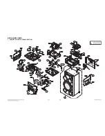
Page 66: ...3 77 3 78 2 MAIN P C BOARD TOP VIEW ...

Page 67: ...3 79 3 80 MAIN P C BOARD BOTTOM VIEW ...

Page 68: ...3 81 3 82 3 TOP FRONT P C BOARD TOP VIEW ...

Page 69: ...3 83 3 84 TOP FRONT P C BOARD BOTTOM VIEW ...

Page 70: ...3 85 3 86 4 JACK RMC P C BOARD TOP VIEW BOTTOM VIEW 5 FRONT LED P C BOARD TOP VIEW BOTTOM VIEW ...

Page 71: ...Assembly Disc 4 3 1 1 1 Plate Clamp 4 3 1 1 2 Magnet Clamp 4 3 1 1 3 Clamp Upper 4 3 2 Tray Disc 4 3 3 Base Assembly Sled 4 4 3 1 Gear Feed 4 4 3 2 Gear Middle 4 4 3 3 Gear Rack 4 4 4 Rubber Rear 4 4 5 Frame Assembly Up Down 4 5 6 Belt Loading 4 5 7 Gear Pulley 4 5 8 Gear Loading 4 5 9 Guide Up Down 4 5 10 PWB Assembly Loading 4 5 11 Base Main 4 5 DECK MECHANISM EXPLODED VIEW DM19AC 4 6 ...

Page 72: ...3 1 2 7 12 13 14 15 16 17 1 2 3 4 5 6 7 8 9 10 11 12 13 14 15 16 17 18 Main Base Clamp Assembly Disc Plate Clamp Magnet Clamp Clamp Upper Tray Disc Base Assembly Sled Gear Feed Gear Middle Gear Rack Rubber Rear Frame Assembly Up Down Belt Loading Gear Pulley Gear Loading Guide Up Down PWB Assembly Loading Base Main 4 Screws 1 Connector 1 Locking Tabs 1 Screw 1 Screw 1 Locking Tab 1 Locking Tab 1 L...

Page 73: ...ate Clamp 1 1 2 Magnet Clamp 1 1 3 Clamp Upper 2 Tray Disc Fig 4 2 1 Insert and push a Driver in the emergency eject hole A at the right side or put the Driver on the Lever B of the Gear Emergency and pull the Lever B in direction of arrow so that the Tray Disc is ejected about 15 20mm 2 Pull the Tray Disc until it is separated from the Base Main completely Fig 4 2 TRAY DISC BASE MAIN LEVER BASE M...

Page 74: ...d 3 2 Gear Middle 3 3 Gear Rack 4 Rubber Rear Fig 4 3 BASE PU RUBBER DAMPER RUBBER DAMPER RUBBER DAMPER Distinguish upper and lower sides Assemble with care Distinguish upper and lower sides Assemble with care RUBBER DAMPER Fig 4 3 S2 S2 S2 S2 GEAR RACK GENERAL PICK UP ASSEMBLY SPINDLE MOTOR ASSEMBLY ...

Page 75: ...he Base Main 8 Gear Loading Fig 4 4 9 Guide Up Down Fig 4 4 1 Move the Guide Up Down in direction of arrow A as Fig A 2 Push the Locking Tab L5 down and then lift up the Guide Up Down to separate it from the Base Main Note When reassembling place the Guide Up Down as Fig C and move it in direction arrow B until it is locked by the Locking Tab L5 And confirm the Guide Up Down as Fig A 10 PWB Assemb...

Page 76: ...4 6 DECK MECHANISM EXPLODED VIEW DM19AC 1439 A001 1002 1005 1001 1003 1004 1026 1043 A005 1016 1013 1015 1020 1439 1018 1019 1012 A006 1045 1049 1437 1437 1024 1024 1024 1024 1437 1011 1030 ...

Reviews: