background image

SERVIC

E
MANUA

L

MODEL

:

TCH-M550

DETACHABLE FRONT
PANEL CAR CD RECEIVER

SERVICE MANUAL

MODEL : 

TCH-M550

CAUTION

BEFORE SERVICING THE UNIT, READ THE “SAFETY PRECAUTIONS”
IN THIS MANUAL.

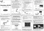
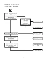
Summary of Contents for TCH-M550

Page 1: ...SERVICE MANUAL MODEL TCH M550 DETACHABLE FRONT PANEL CAR CD RECEIVER SERVICE MANUAL MODEL TCH M550 CAUTION BEFORE SERVICING THE UNIT READ THE SAFETY PRECAUTIONS IN THIS MANUAL ...

Page 2: ... 1 CD PART TROUBLESHOOTING GUIDE 2 3 WAVEFORMS OF MAJOR CHECK POINT 2 11 INTERNAL BLOCK DIAGRAM of ICs 2 13 BLOCK DIAGRAM 2 25 MAIN SCHEMATIC DIAGRAM 2 27 FRONT SCHEMATIC DIAGRAM 2 29 CDP SCHEMATIC DIAGRAM 2 31 PRINTED CIRCUIT DIAGRAM 2 33 SECTION 3 CABINET MAIN CHASSIS MECHANISM EXPLODED VIEW 3 1 SECTION 4 REPLACEMENT PARTS LIST 4 1 CONTENTS ...

Page 3: ...itive lead Always remove the test instrument ground lead last 1 The service precautions are indicated or printed on the cabinet chassis or components When servicing follow the printed or indicated service precautions and service materials 2 The Components used in the unit have a specified conflammability and dielectric strength When replacing any components use components which have the same ratin...

Page 4: ...harges sufficient to damage ESD devices 5 Do not use freon propelled chemicals These can generate electrical charges sufficient to damage ESD devices 6 Do not remove a replacement ESD device from its protective package until immediately before you are ready to install it Most replacement ESD devices are packaged with leads electrically shorted together by conductive foam aluminum foil or comparabl...

Page 5: ...Hz 520 1 620kHz Intermediate frequency 10 8MHz 450kHz Usable sensitivity 12dBµV 32dBµV Signal to noise ratio 55dB 45dB 3 COMPACT DISC SECTION Frequency response 40Hz 20kHz Channel separation 50dB 1kHz Signal to noise ratio 60dB 4 AUDIO SECTION Maximum output power 50W x 4 Speaker impedance 4Ω x 4 or 8Ω x 4 NOTE The design and specifications are subject to change without notice in the sourse of pro...

Page 6: ...udio output supplied Check power supply circuitry Q260 Q380 Q381 IC401 Pin3 IC201 Pin2 Check loading supply circuitry Q350 Q351 PN505 IC401 Pin1 Check laser circuitry Q501 IC502 Check focusing circuitry Q501 IC502 Check DISC Check tracking servo circuitry Q501 IC502 Check audio circuitry IC502 IC601 IC801 OK YES YES YES YES YES YES NO NO NO NO NO 1 No Power ...

Page 7: ...e X401 C413 C414 defective Q260 PN401 front PCB pattern defective IC401 Pin 66 67 88 89 front PCB pattern defective IC901 Surrounding circuit PCB pattern defective Is u com IC401 reset circuit normal Pin10 Is u com IC401 keyin Pin9 37 5volt input Is u com IC401 Pin 66 67 88 89 output waveform normal Is IC901 Com1 Com2 Com3 output waveform normal Display LCD connector defective Is u com IC401X1 X2 ...

Page 8: ... 2 3 ...

Page 9: ... 2 4 ...

Page 10: ... 2 5 ...

Page 11: ... 2 6 ...

Page 12: ... 2 7 ...

Page 13: ... 2 8 ...

Page 14: ... 2 9 ...

Page 15: ... 2 10 ...

Page 16: ...M CN503 1 9 2 1 1 8 20 during normal play 2 SLED DRIVE AND MOTOR WAVEFORM IC504 pin5 1 4 when focus search 3 FOCUS DRIVE AND MOTOR WAVEFORM R5 1 3 IC504 pin 1 5 When focus search failed or there is no disc on the tray There is disc on tray and focus search success ...

Page 17: ...SPINDLE DRIVE AND MOTOR WAVEFORM IC504 pin6 1 2 when TOC reading 5 TRACK DRIVE AND MOTOR WAVEFORM R508 IC504 pin23 during normal play 6 RF TRACKING AND FOCUS ERROR WAVEFORM IC502 pin8 2 1 23 during normal play ...

Page 18: ..._CE O PPLL_CLK O PPLL_DO O PPLL_DI I PFRT_CLK O PFRT_DO O N C AVREF1 N C N C AVSS N C PVOLB I PVOLA I PKEY2 I PKEY1 I PLVL_MTR I PS_MTR I N C AVREF0 AVDD N C PDSP_IDRF I PDSP_ORST O PDSP_OCEN O N C N C V DD 9 8304 MHz 9 8304 MHz V SS 32 768 KHz 32 768 KHz RESET PRDS_CLK I PCD_IWRQ I PCDC_DI I PRMC I N C N C N C V SS N C N C N C N C N C N C N C N C PACC I PANT O PFRT_DET I PFRT_RES O PFRT_CE O PCD_...

Page 19: ...E I O O N ch To tuner pack AF mute output 27 P94 PCD_IDO I O O N ch To CD changer data output 28 P95 N C I O O N ch Not to be used Open 29 P120 RTP0 PDRV_OPS I O O CMOS In MD motor driver s power save command output 30 P121 RTP1 PDRV_OMUTE I O O CMOS In MD all motor s output cut off command output 31 P122 RTP2 N C I O O CMOS Not to be used Open 32 P123 RTP3 PDSP_IDRF I O I Focusing OK signal input...

Page 20: ...rep indigater s signal or SD signal input 80 P84 A4 PRDS_DI I O I From tuner pack RDS data input 81 P85 A5 PORT_IN0 I O I For diode option check signal 1 or 2 input 0 82 P86 A6 PORT_IN1 I O I For diode option check signal 1 or 2 input 1 83 P87 A7 PORT_IN2 I O I For diode option check signal 1 or 2 input 2 84 P40 AD0 PORT_OUT0 I O O CMOS For diode option check signal 1 output 85 P41 AD1 PORT_OUT1 I...

Page 21: ... IC501 MN6627933 1 PORT ASSIGNMENT 2 16 ...

Page 22: ... 2 17 2 Block Diagram ...

Page 23: ...l output absolute value 30 SPPOL O Spindle drive signal output polarity 31 TRVP O Traverse drive signal output positive polarity 32 TRVM O Traverse drive signal output negative polarity 33 TRVP2 O Traverse drive signal output 2 positive polarity 34 TRVM2 O Traverse drive signal output 2 negative polarity 35 TRP O Tracking drive signal output positive polarity 36 TRM O Tracking drive signal output ...

Page 24: ...ignal output 78 PMCK O 88 2 kHz clock signal output 79 TX O Digital audio interface signal output 80 FLAG O Flag signal output 81 NRST I LSI reset signal input 82 NTEST I Test mode setting input 83 DVSS3 I Ground 3 for digital circuits 84 X1 I Crystal oscillator circuit input 85 X2 O Crystal oscillator circuit output 86 IOVDD2 I Power supply 2 for digital I O 87 DVDD2 I Power supply 2 for internal...

Page 25: ...KE CS RAS CAS WE L U DQM LDQM LWCBR LCAS Bank Select LWE LDQM DQI Data Input Regidter 512K x 16 512K x 16 Column Decoder Latency Burst Length Programming Register Timing Register Address Register Row Decoder LCBR LRAS Sense AMP I O Control Output Buffer Col Buffer Row Buffer Refresh Counter ...

Page 26: ...he positive going edge of the CLK with CAS low Enables column access WE Write Enable Enables write operation and row precharge Latches data in starting from CAS WE active L U DQM Data Input Output Mask Makes data output Hi Z tSHZ after the clock and masks the output Blocks data input when L U DQM active DQ0 15 Data Input Output Data inputs outputs are multiplexed on the same pins VDD VSS Power Sup...

Page 27: ... 2 22 IC505 AMC1117 BLOCK DIAGRAM ...

Page 28: ... Control LIN2 LIN2 LIN1 LOUT LIN LOUD_L BOUT_L BIN_L TREB_L LFOUT Mute Mute Mute Mute Speaker ATT Speaker ATT Speaker ATT Speaker ATT LROUT CLK DATA DGND RFOUT RROUT LIN1 2 11 10 9 13 14 15 17 16 12 19 18 4 25 23 28 27 26 24 22 3 1 7 6 8 21 20 5 Supply Bass Serial Bus Decoder Latches Bass Treble Treble Voume Loudness Voume Loudness ...

Page 29: ... 2 24 IC801 TA8275H IC901 LC75811 ...

Page 30: ... DRIVE IC BA5810FM DSP IC MN6627933 RF IC AN22004A OP AMP S4560 RADIO VCC Q350 ZD313 LINE SW E VOLUME 9 4V REG Q360 ZD361 POWER 5V Q282 Q283 7 5V REG Q310 Q351 3 3V REG IC805 U COM uPD789166 KEY MATRIX RESISTOR RADER RESET IC201 5V CONVERT Q260 ZD261 D201 REG 10V IC403 LCD DRIVER LC75811W LCD DISPLAY PHONE MUTE Q280 281 ACC DETECTOR Q230 D231 D232 REMOTE CONTROL Q320 321 ANT CONTROL Q390 391 POWER...

Page 31: ... SCHEMATIC DIAGRAM MAIN SCHEMATIC DIAGRAM 2 27 2 28 ...

Page 32: ...2 29 2 30 FRONT SCHEMATIC DIAGRAM ...

Page 33: ...2 31 2 32 CDP SCHEMATIC DIAGRAM ...

Page 34: ...2 33 2 34 LED P C BOARD LED P C BOARD FRONT P C BOARD SOLDER SIDE FRONT P C BOARD COMPONENT SIDE PRINTED CIRCUIT DIAGRAM ...

Page 35: ... MAIN P C BOARD 2 35 2 36 ...

Page 36: ...2 37 2 38 CDP P C BOARD CDP P C BOARD ...

Page 37: ...2 278 271 276 262 250 252 269 253 254 A47 290 450 450 450 450 273 453 A43 251 284 A41 261 264 256 255 263 260 259 258 261 CAUTION Exposed blade will cause severe injury NOTE Refer to SECTION 4 REPLACEMENT PARTS LIST in order to look for the part number of each part SECTION 3 CABINET MAINCHASSIS MECHANISM ...

Reviews: