1
dc1369af
DEMO MANUAL DC1369A
Description
LTC2262-14/-12, LTC2261-14/-12,
LTC2260-14/-12, LTC2259-14/-12, LTC2258-14/-12, LTC2257-14/-12,
LTC2256-14/-12, 14/12-Bit, 25Msps to 150Msps ADCs
Demonstration circuit 1369A supports a family of
14/12-bit 25Msps to 150Msps ADCs. Each assembly
features one of the following devices: LTC2262-14 or
LTC2262-12, LTC2261-14, LTC2261-12, LTC2260-14,
LTC2260-12, LTC2259-14, LTC2259-12, LTC2258-14,
LTC2258-12, LTC2257-14, LTC2257-12, LTC2256-14,
LTC2256-12, high speed, high dynamic range ADCs.
Demonstration circuit 1369A supports the LTC2261 family
DDR LVDS output mode. This family of ADCs is also sup-
ported by demonstration circuit 1370A, which is compatible
with CMOS and DDR CMOS output modes.
performance summary
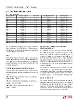
Several versions of the 1369A demo board supporting the
LTC2261 14/12-bit series of A/D converters are listed in
Table 1. Depending on the required resolution and sample
rate, the DC1369A is supplied with the appropriate ADC.
The circuitry on the analog inputs is optimized for analog
input frequencies from 5MHz to 170MHz. Refer to the
data sheet for proper input networks for different input
frequencies.
Design files for this circuit board are available at
http://www.linear.com/demo
L
, LT, LTC, LTM, Linear Technology and the Linear logo are registered trademarks and PScope
and QuikEval are trademarks of Linear Technology Corporation. All other trademarks are the
property of their respective owners.
(T
A
= 25°C)
Table 1
PARAMETER
CONDITION
VALUE
Supply Voltage – DC1369A
Depending on sampling rate and the A/D converter
provided, this supply must provide up to 250mA
Optimized for 3.6V
3.5V
↔
6.0V Min/Max
Analog Input Range
Depending on SENSE Pin Voltage
1V
P-P
to 2V
P-P
Logic Input Voltages
Minimum Logic High
1.3V
Maximum Logic Low
0.6V
Logic Output Voltages (Differential)
Nominal Logic Levels (100Ω Load, 3.5mA Mode)
350mV/1.25V Common Mode
Minimum Logic Levels (100Ω Load, 3.5mA Mode)
247mV/1.25V Common Mode
Sampling Frequency (Convert Clock Frequency)
See Table 1
Convert Clock Level
Single-Ended Encode Mode (ENC – Tied to GND)
0V to 3.6V
Convert Clock Level
Differential Encode Mode (ENC – Not Tied to GND)
0.2V to 3.6V
Resolution
See Table 1
Input Frequency Range
See Table 1
SFDR
See Applicable Data Sheet
SNR
See Applicable Data Sheet


