1
dc1513bf
DEMO MANUAL DC1513B
DESCRIPTION
LTM9004
14-Bit Direct Conversion
Receiver Subsystem
Demonstration circuit 1513 is an evaluation board featuring
Linear Technology Corporation’s LTM
®
9004 14-bit direct
conversion receiver subsystem. DC1513 demonstrates
good circuit layout techniques and recommended external
circuitry for optimal system performance.
DC1513 comes with Linear Technology’s 14-bit LTM9004
receiver subsystem installed. The board includes out-
put CMOS buffers. DC1513 plugs into the DC890 data
QUICK START PROCEDURE
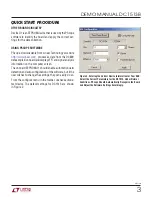
acquisition demo board and the output can be easily ana-
lyzed with Linear Technology’s PScope™ data processing
software, which is available for no charge on our website at
http://www.linear.com/software
.
Design files for this circuit board are available at
http://www.linear.com/demo
Validating the performance of the LTM9004 is simple
with DC1513, and requires only two input sources, a
clock source, a computer, and a lab power supply. Refer
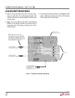
to Figure 1 for proper board evaluation equipment setup
and follow the procedure below:
1. Connect the power supply as shown in Figure 1. There
are onboard low noise voltage regulators that provide
the two supply voltages for the DC1513. The entire
board and all components share a common ground.
The power supply should still be a low noise lab power
supply capable of supplying at least 0.5A at 5VDC, and
1A at 3VDC.
2. Provide an encode clock to the ADC via SMA connec-
tor J7. Use a low-phase-noise clock source such as
a filtered RF signal generator or a high quality clock
oscillator.
NOTE:
Similar to having a noisy input, a high jitter (phase
noise) encode clock will degrade the signal-to-noise
ratio (SNR) of the system.
Table 2. DC1513 Connectors and Jumpers
REFERENCE
FUNCTION
J3 (SHDN)
Enables/Disables the ADC. Default Is ON.
J4 (MODE)
Output Format and Clock Duty Stabilizer Pin.
Default Is VDD.
J5 (SHDN_AMP)
Enables/Disables the Amplifiers. Default Is ON.
J6 (LO)
Board LO Signal Input. Impedance Matched to
50Ω for Use with Lab Signal Generators.
J7 (CLK)
Board Clock Input. Impedance Matched to 50Ω.
Drive with a Low-Phase-Noise Clock Oscillator or
Filtered Sine Wave Signal Source.
J8 (MIXER ENABLE) Enables/Disables the RF Mixer. Default Is ON.
J11 (RF)
Board RF Signal Input. Impedance Matched to
50Ω for Use with Lab Signal Generators.
TP1 (SENSE_I)
Reference Input to Adjust the Full-Scale Range of
the DC1513, I-Channel. Default Is VDD.
TP2 (GND)
DC Ground.
TP4 (GND)
DC Ground.
TP5 (3V)
DC Supply Input (3VDC).
TP7 (5V)
DC Supply Input (5VDC).
TP8 (GND)
DC Ground.
TP12 (SENSE_Q)
Reference Input to Adjust the Full-Scale Range of
the DC1513, Q-Channel. Default Is VDD.
Table 1. DC1513B Variants
DC1513B VARIANTS
RESOLUTION
MAXIMUM SAMPLE RATE
BASEBAND BANDWIDTH
1513B-AA
14-Bit
125Msps
DC - 1.92MHz
1513B-AB
14-Bit
125Msps
DC - 4.42MHz
1513B-AC
14-Bit
125Msps
DC - 9.42MHz
1513B-AD
14-Bit
125Msps
DC - 20MHz
L
, LT, LTC, LTM, Linear Technology and the Linear logo are registered trademarks and PScope
is a trademark of Linear Technology Corporation. All other trademarks are the property of their
respective owners.


