background image

1

dc1721bf

DEMO MANUAL 

DC1721B-A/DC1721B-B 

 DESCRIPTION

LTC4000EGN(-1)/LTC3789EGN

14.6V, 5A Battery Charger with 

6V

IN

 to 36V

IN

 Buck-Boost Converter

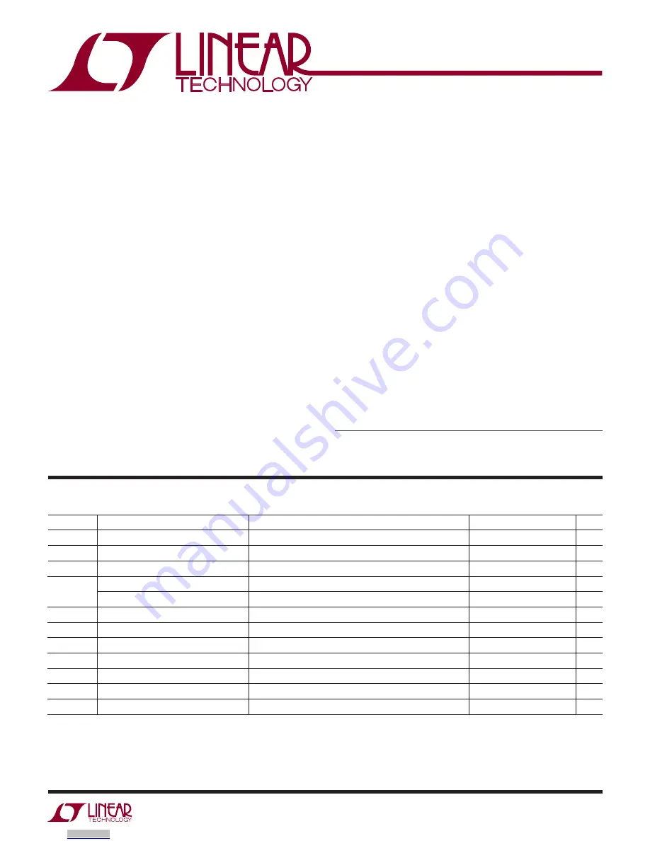
Demonstration circuit 1721B is a 14.6V, 5A battery charger 
and PowerPath™ manager with 6V

IN

 to 36V

IN

 buck-boost 

converter featuring the LTC4000/LTC3789, targeted at 
4-cell LiFePO

4

 applications. The output of this demo board 

was specifically tailored for a Tenergy 10A-hour battery, 
P/N 30207. Other voltages can be set by changing ROFB2 
and RBFB2. The desired nominal voltage can be accurately 
trimmed by using trim resistors R42 and R43. For example, 
for 14.4V battery float voltage, change ROFB2 and RBFB2 
to 86.6k, and add 7.5M at R42 and R43 for greater set 
point accuracy.

This circuit was designed to demonstrate the high levels of 
performance, efficiency, and small solution size attainable 
using these ICs in a buck-boost converter battery charger, 
intelligent PowerPath manager, and power supply. It oper-
ates at 400kHz and produces a regulated 5A/14.6V battery 
charger output as well as a system output of up to 6.25A 
from an input voltage range of 6V to 36V: suitable for a 

L

, LT, LTC, LTM, Linear Technology and the Linear logo are registered trademarks and 

PowerPath is a trademark of Linear Technology Corporation. All other trademarks are the 
property of their respective owners.

 PERFORMANCE SUMMARY

wide variety of portable applications including instruments, 
industrial equipment, power tools, and computers. It has 
a total footprint area of 12.4cm

2

 (3.6cm

2

 for the LTC4000 

circuit only). Synchronous rectification helps to attain 
efficiency exceeding 96% at full load and nominal input.

DC1721B-A:

 The LTC4000 has an input current limit/

regulation loop that prevents overloading sources with 
limited output capability.

DC1721B-B:

 The LTC4000-1 instead has an input voltage 

regulation loop for Maximum Power Point (MPP) control. 
MPP control extracts near maximum power from high 
impedance sources such as solar panels, wind turbines, 
or fuel cells.

Design files for this circuit board are available at 
http://www.linear.com/demo

Specifications are at T

A

 = 25°C

SYMBOL

PARAMETER

CONDITIONS

MIN

TYP

MAX

UNITS

V

IN

Input Supply Range

6

36

V

V

IN-MP

1

Input Regulation Voltage

This Is the Input Voltage Lower Limit Set by the LTC4000-1

11.85

V

I

IN

2

Input Current Limit

11

A

V

FLOAT

Battery Float Voltage 

14.4

14.6

14.8

V

Output Regulation

Line and Load (6V to 36V, 0A to 5A)

±0.05

%

I

BAT

Battery Charge Current 

5.0

A

V

OUT-SYS

System Output Voltage 

12.3

14.6

15.5

V

I

OUT-SYS

System Output Current Range

0

6.25

A

F

SW

Switching (Clock) Frequency

400

kHz

V

OUT-SYS P-P

System Output Ripple

V

IN

 = 24V, I

OUT-SYS

 = 5A (20MHz BW)

50

mV

P-P

P

OUT

/P

IN

System Output Efficiency (See Figure 3) V

IN

 = 24V, I

OUT-SYS

 = 5A

96.5

%

Approximate Size

Component Area 

×

 Top Component Height

12.4cm

2


×

 0.40cm

1

 DC1721B-B (LTC4000-1) Only,

2

 DC1721B-A (LTC4000) Only

Downloaded from

Arrow.com.

Summary of Contents for DC1721B-A

Page 1: ...portableapplicationsincludinginstruments industrial equipment power tools and computers It has a total footprint area of 12 4cm2 3 6cm2 for the LTC4000 circuit only Synchronous rectification helps to attain efficiency exceeding 96 at full load and nominal input DC1721B A The LTC4000 has an input current limit regulation loop that prevents overloading sources with limited output capability DC1721B ...

Page 2: ...s no output temporarily disconnect the load to make sure that the load is not set too high 8 OncetheproperVOUT SYSisagainestablished adjust the load and or source within the operating range and observe the output voltage regulation ripple voltage efficiency input and output current limit and other desired parameters 9 Turn off the power at the input 10 Connect the output load and meters to the BAT...

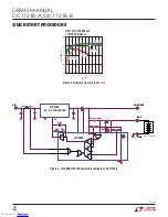
Page 3: ...EMO MANUAL DC1721B A DC1721B B QUICK START PROCEDURE Figure 1 Proper Measurement Equipment Setup Figure 2 Proper Noise Measurement Setup Downloaded from Arrow com Downloaded from Arrow com Downloaded from Arrow com ...

Page 4: ... LTC4000 Gm Gm Gm Gm LTC3789 NOT ON THE BOARD GND GND RC1 RC1 CC1 CC1 VOUT SYS VOUT SYS BAT BAT VIN VIN 10nF 10nF CC2 CC2 Figure 3 Efficiency from VIN to VOUT SYS DC1721A LTC4000 and LTC3789 Efficiency IOUT A 0 5 EFFICIENCY 100 95 85 90 80 2 5 4 5 1 5 3 5 5 5 VIN 36V VIN 24V VIN 6V VIN 15V Downloaded from Arrow com Downloaded from Arrow com Downloaded from Arrow com Downloaded from Arrow com ...

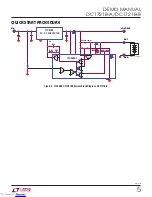
Page 5: ...A10 A8 A9 Rsense charge DC DC CONVERTER ITH LTC4000 1 Gm Gm Gm Gm LTC3789 NOT ON THE BOARD GND GND RC1 RC1 CC1 CC1 VOUT SYS VOUT SYS BAT BAT VIN VIN 10nF 10nF CC2 CC2 QUICK START PROCEDURE Downloaded from Arrow com Downloaded from Arrow com Downloaded from Arrow com Downloaded from Arrow com Downloaded from Arrow com ...

Page 6: ...KY 40V 2A SMA DIODES ZETEX B240A 13 F 21 1 D9 DIODE ZENER 3V 500MW SOD 323 DIODES ZETEX BZT52C3V0S 7 F 22 1 F1 FUSE 6 3A 32V T LAG 1206 SMD COOPER BUSSMAN 3216TD6 3 R 23 1 L1 INDUCTOR 4 7μH TOKO FDA1254 4R7M 24 2 Q2 Q4 MOSFET N Chan 40V POWERPAK 8 VISHAY SiR422DP T1 GE3 25 2 Q3 Q5 MOSFET N Chan 20V POWERPAK 8 VISHAY SiR496DP T1 GE3 26 2 Q6 Q7 MOSFET P Chan 30V POWERPAK 8 VISHAY Si7135DP T1 GE3 27 ...

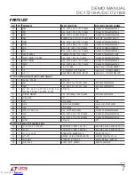
Page 7: ...al Demo Board Circuit Components 57 0 C3 C23 C26 C27 OPT 1210 58 1 C33 CAP X5R 4 7μF 10V 20 0603 AVX 0603ZD475MAT2A 59 1 CBAT CAP X5R 2 2μF 25V 20 0805 AVX 08053D225MAT2A 60 0 CF1 CC1 R6 C7 C8 C11 R12 R22 R27 R30 R38 R43 R53 R61 R62 CNTC CF CCX OPT 0603 OPT 61 2 CIIMON CIBMON CAP C0G 1000pF 25V 5 0603 AVX 06033A102JAT2A 62 0 CIN3 CIN4 OPT 63 0 D11 OPT SOD323 OPT 64 1 LED2 LED DUAL RED GREEN LiteOn...

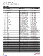
Page 8: ...C3V0S 7 F 21 1 D10 DIODE ZENER 5 6V 500MW SOD 123 DIODES ZETEX BZT52C5V6 7 F 22 1 F1 FUSE 6 3A 32V T LAG 1206 SMD COOPER BUSSMAN 3216TD6 3 R 23 1 L1 INDUCTOR 4 7μH TOKO FDA1254 4R7M 24 2 Q2 Q4 MOSFET N Chan 40V POWERPAK 8 VISHAY SiR422DP T1 GE3 25 2 Q3 Q5 MOSFET N Chan 20V POWERPAK 8 VISHAY SiR496DP T1 GE3 26 2 Q6 Q7 MOSFET P Chan 30V POWERPAK 8 VISHAY Si7135DP T1 GE3 27 2 Q8 Q9 MOSFET SMALL SIGNA...

Page 9: ... DC1721B B Additional Demo Board Circuit Components 58 0 C3 C23 C26 C27 OPT 1210 59 1 C33 CAP X5R 4 7μF 10V 20 0603 AVX 0603ZD475MAT2A 60 1 CBAT CAP X5R 2 2μF 25V 20 0805 AVX 08053D225MAT2A 61 0 CF1 CC1 R6 C7 C8 C11 R12 R22 R27 R30 R38 R43 R53 R61 R62 CNTC CF CCX OPT 0603 OPT 62 2 CIIMON CIBMON CAP C0G 1000pF 25V 5 0603 AVX 06033A102JAT2A 63 0 CIN3 CIN4 OPT 64 0 D11 OPT SOD323 OPT 65 1 LED2 LED DU...

Page 10: ...HOWEVER IT REMAINS THE CUSTOMER S RESPONSIBILITY TO VERIFY PROPER AND RELIABLE OPERATION IN THE ACTUAL APPLICATION COMPONENT SUBSTITUTION AND PRINTED CIRCUIT BOARD LAYOUT MAY SIGNIFICANTLY AFFECT CIRCUIT PERFORMANCE OR RELIABILITY CONTACT LINEAR TECHNOLOGY APPLICATIONS ENGINEERING FOR ASSISTANCE THIS CIRCUIT IS PROPRIETARY TO LINEAR TECHNOLOGY AND SCHEMATIC SUPPLIED FOR USE WITH LINEAR TECHNOLOGY ...

Page 11: ...ONS HOWEVER IT REMAINS THE CUSTOMER S RESPONSIBILITY TO VERIFY PROPER AND RELIABLE OPERATION IN THE ACTUAL APPLICATION COMPONENT SUBSTITUTION AND PRINTED CIRCUIT BOARD LAYOUT MAY SIGNIFICANTLY AFFECT CIRCUIT PERFORMANCE OR RELIABILITY CONTACT LINEAR TECHNOLOGY APPLICATIONS ENGINEERING FOR ASSISTANCE THIS CIRCUIT IS PROPRIETARY TO LINEAR TECHNOLOGY AND SCHEMATIC SUPPLIED FOR USE WITH LINEAR TECHNOL...

Page 12: ...E OTHER FOR ANY INDIRECT SPECIAL INCIDENTAL OR CONSEQUENTIAL DAMAGES The user assumes all responsibility and liability for proper and safe handling of the goods Further the user releases LTC from all claims arising from the handling or use of the goods Due to the open construction of the product it is the user s responsibility to take any and all appropriate precautions with regard to electrostati...

Reviews: