


LT8302
1
8302fb
For more information
www.linear.com/LT8302
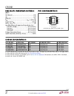
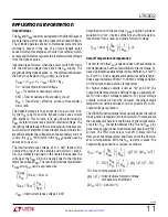
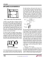
Typical applicaTion
FeaTures
DescripTion
42V
IN
Micropower No-Opto
Isolated Flyback Converter
with 65V/3.6A Switch
The
LT
®
8302
is a monolithic micropower isolated flyback
converter. By sampling the isolated output voltage directly
from the primary-side flyback waveform, the part requires
no third winding or opto-isolator for regulation. The output
voltage is programmed with two external resistors and a
third optional temperature compensation resistor. Bound-
ary mode operation provides a small magnetic solution with
excellent load regulation. Low ripple Burst Mode operation
maintains high efficiency at light load while minimizing the
output voltage ripple. A 3.6A, 65V DMOS power switch
is integrated along with all the high voltage circuitry and
control logic into a thermally enhanced 8-lead SO package.
The LT8302 operates from an input voltage range of 2.8V
to 42V and delivers up to 18W of isolated output power.
The high level of integration and the use of boundary
and low ripple burst modes result in a simple to use, low
component count, and high efficiency application solution
for isolated power delivery.
2.8V to 32V
IN
/5V
OUT
Isolated Flyback Converter
applicaTions
n
2.8V to 42V Input Voltage Range
n
3.6A, 65V Internal DMOS Power Switch
n
Low Quiescent Current:
106µA in Sleep Mode
380µA in Active Mode
n
Quasi-Resonant Boundary Mode Operation at
Heavy Load
n
Low Ripple Burst Mode
®
Operation at Light Load
n
Minimum Load < 0.5% (Typ) of Full Output
n
No Transformer Third Winding or Opto-Isolator
Required for Output Voltage Regulation
n
Accurate EN/UVLO Threshold and Hysteresis
n
Internal Compensation and Soft-Start
n
Temperature Compensation for Output Diode
n
Output Short-Circuit Protection
n
Thermally Enhanced 8-Lead SO Package
n
Isolated Automotive, Industrial, Medical Power
Supplies
n
Isolated Auxiliary/Housekeeping Power Supplies
L
, LT, LTC, LTM, Linear Technology, the Linear logo and Burst Mode are registered trademarks
of Linear Technology Corporation. All other trademarks are the property of their respective
owners. Protected by U.S. Patents, including 5438499, 7463497, 7471522.
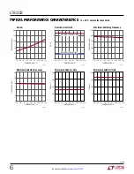
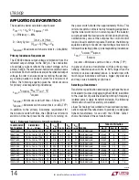
Efficiency vs Load Current
V
IN
LT8302
SW
9µH
V
IN
2.8V TO 32V
3:1
1µH
R
FB
R
REF
EN/UVLO
470pF
10µF
1µF
220µF
10mA TO 1.1A (V
IN
= 5V)
10mA TO 2.0A (V
IN
= 12V)
10mA TO 2.9A (V
IN
= 24V)
V
OUT
–
39Ω
154k
•
•
115k
10k
8302 TA01a
GND
INTV
CC
TC
V
OUT
+
5V
LOAD CURRENT (A)
0
EFFICIENCY (%)
80
85
90
1.5
2.5
8302 TA01b
75
70
0.5
1.0
2.0
3.0
65
60
V
IN
= 5V
V
IN
= 12V
V
IN
= 24V
FRONT PAGE APPLICATION


